This thread has been locked.

If you have a related question, please click the "Ask a related question" button in the top right corner. The newly created question will be automatically linked to this question.

DAC0800: Trying bipolar DAC operation with a +12/-12 supply and a +8Vref

Part Number: DAC0800
Other Parts Discussed in Thread: DAC0802, , LM324

Hi,

I am trying to debug a situation where I re-created a circuit fundamentally identical to the one listed in your document/datasheet SNAS538C ( DAC0800, DAC0802) page 10 figure 23 with the following modifications :

- the V+ is 12V - the V- is -12V

- the opAMP is an LM324 ( powered as well at +12V -12V )

- the Vref first been tried at 8.0V

- the resistors, to meet the 2mA requirement been changed from 5KOhm to 4KOhm

- Input are TTL level guaranteed to match the requirements ( i.e. Voh > 2.0 V and Vol < 0.8 V)

- VLC been set to 0V ( for TTL input )

In those conditions I can't make the DAC work at all, no matter the digital inputs there appear to be absolutely no variation in the output ( which seems to be stuck at 11.89 V about ).

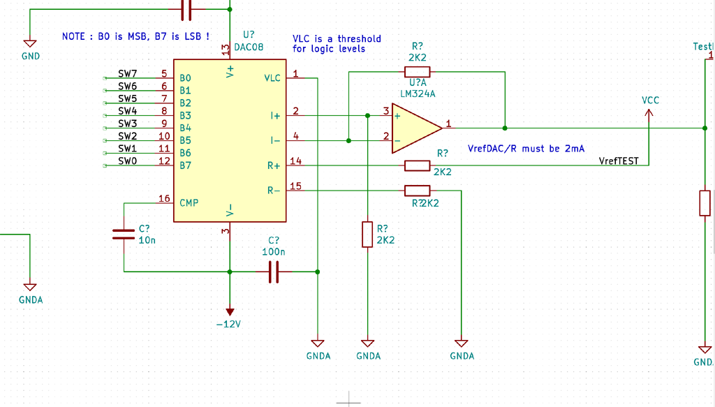
Then I tried a "test rig" to try to nail down the problem ( see attached schematic , VCC  is set to 5V , so Vref is 5V ) but then again the DAC in those conditions seems simply not work at all.

I can't figure out why.

At this point some things are not very clear in the Datasheet, all the examples seems to show that Vref is always set at +0V, can it be set at any different value ?

Is that a VrefMin / VrefMax value that has to be respected and/or some relationships between Vref and Vsupply ?

The datasheet seems to mention the DAC0800 can work with a supply from -/+ 4.5 V up to a max of +/- 18V so I assume there should be no problems in working with +/- 12V ?

Thanks in advance for any help, it's really puzzling me.

TestRig.pdf

Cheers. Ivan Z.

  • Hi,

    The very basic fact that you got your output railed out indicates some issues with LM324.

    Can you please verify the output current node rather than the op amp output, I believe you followed fig 23, in that case please measure the voltage across the resistor from non inverting terminal to ground.

    Also please share the schematics, Its very difficult for us to look at board and understand what is the actual circuit you built.

    Regards.

    AK

  • Hi,

    just a quick reply, my schematics are in the attached PDF file, I can try to make a PNG print and re-upload it but they should be in the post.

    [edit] - here I converted it into a PNG, maybe that's easier to see.

  • Hi Ivan,

    Circuit wise I am not seeing any issues.

    whats the VCC level? tested with 5V? 

    1. Can you feed all digital inputs logic low and probe voltage across R7?

    Regards,

    AK 

  • Hi,

    I re-checked again all connections and they match the schematics so it's puzzling me even more.

    I am measured here between GND and pin 4 of the DAC so basically across the resistor the the non inverting input and ground.

    I got the following results :

    MSB .. LSB   Volt

    0000 0000   -6.79

    1111 1111   -5.81


    1000 0000   -6.51

    1100 0000   -6.25

    1110 0000   -6.03

    1111 0000   -5.87

    1111 1000   -5.93

    1111 1100   -5.92

    1111 1111   -5.85

    And then

    1000 0000   -6.51

    0100 0000   -6.59

    0010 0000   -6.63

    0001 0000   -6.69

    0000 1000   -6.87

    0000 0100   -6.83

    0000 0010   -6.75

    0000 0001   -6.80

    Quite strange is it ?

  • Hi Ivan,

    Is this measurement with Vref  = 4V or 5V? Please clarify.

    for all Zero, you got -6.79V and full code its -5.81V?

    Can you please disconnect the op amp and test only with resistors to ground on both Iout? I just want to isolate the problem.

    Regards,

    AK

  • Hi,

    as per schematics the Vref of the TestRig is at +5V .

    Now removing the op-amp and connecting the two test pins togheter has the effect of short circuiting Rload ( and putting it at 0 ohm ) leaving pin 2 and pin 4 of the DAC both connected to GND via a 2K2 resistor.

    So basically doing what you say.

    In doing so by measuring between GND and pin 4 I get the following situation : ( my analyser has not big accuracy )

    MSB .. LSB    Volt at pin 4     Volt at pin 2

    0000 0000      0                -4.84

    1111 1111      -4.91            0

    1000 0000      -2.45            -2.41


    0000 0001      -0.02            -4.83

    0000 0010      -0.04            -4.81

    0000 0100      -0.08            -4.77

    0000 1000      -0.15            -4.70

    0001 0000      -0.30            -4.54

    0010 0000      -0.61            -4.24

    0100 0000      -1.22            -3.63

    1000 0000      -2.45            -2.41

    So apart some probably imprecision of my instrument and/or non linearity ( that I am not sure is guarantee at 5V Vref, I think the datasheet mentions 10V to be guaranteed ) it would
    appear that "something works" ?

    Cheers.

    ( re-measured and added the voltages at pin 2 too )

  • Hi,

    You are getting the expected output at IOUT.

    I am assuming you got negative value because you measured between GND and pin 2.  This is the configuration which I have asked you to test,.

    I strongly feel there is some issue with the op amp output. 

    Please check the pads and connections one more time. DAC is working as intended.

    Regards,

    AK

  • Hi,

    later on I'll do a few more tests, as it does happen while looking for things I stumbled across a similar schematics in a schoolbook using precisely the DAC0800 in a very similar configuration, even listing the expected V output for a given digital input.

    BUT .. in their schematics, the +/- pins of the op-am results "inverted" , I mean pin 4 of the dac goes to '-' input, pin 2 of the dac into the '+' input and there's a negative reaction so the output of the op-am is via a 4.7k resistor back to the '-' input of the op-amp.

    This is taken from a schoolbook text titled "Elettronica, le applicazioni" ( Electronics, the applications ) ISBN 88-7019-822-7 page 351 ( lab ) "Exercise 8.6.1" "Practical test of using a D/A converter with a uP" they even use 12V supply but with a 10Vref and they use an LF351 in place of my LM324.

    I begin to wonder if there's a "print error" in the datasheet about the op-amp inputs ?

    Anyway later on I am going to modify/test again .. I can't believe I am finding "the same thing done in 2 completely different ways" one of the two seems to be not working right.

    Cheers.


  • Hi,

    Finally I fixed it, and now I am 90% convinced "there's a print error in the PDF/datasheet".

    After THIS MODIFICATION, compare it to the schematics above, ALL WORKS.

    As you can see it's a minor thing, but this is the kind of values I get after that modification :

    Digital Input Volt

    MSB LSB

    0000 0000 -4.88

    1111 1111 4.88

    0000 0001 -4.85

    0000 0010 -4.81

    0000 0100 -4.73

    0000 1000 -4.58

    0001 0000 -4.27

    0010 0000 -3.66

    0100 0000 -2.44

    1000 0000 0.01

    1000 0001 0.04

    1000 0010 0.08

    1000 0100 0.16

    1000 1000 0.31

    1001 0000 0.62

    1010 0000 1.23

    1100 0000 2.46

    As you can see all now seems to be going as it should, this way works, the other way doesn't, the other way I copied it as it is from the datasheet, I don't know I wonder if "if it's just me" or if it's really a typo.

    But yes, everything else now seems to match expectations/computations so I don't know what to think now, I'll re-check again but I am quite sure or somewhere there's some other error or the datasheet really has a typo ?

    Cheers.

  • Hi Ivan,

    There is no typo in the datasheet. Mistake is in your schematics, if you look at your first schematics, op amp was connected in positive feedback eventually resulted in railing out. That's the reason I have asked you to remove the op amp and test ( I was just giving you a test to understand that :)

    You need to connect pin 4 of the DAC to op amp negative input and have feedback taken to output through the resistor. Pin 2 of the DAC should be connected to positive input and from the same node connect resistor to ground. That's the recommended implementation.

    Anyway you corrected the same and made it work. Also in your DAC symbol pin 4 is shown as I- why is that?

  • Hi,

    I am guessing "that's what you get for doing this kind of work past midnight after a work day".

    I was wondering "how can it work with a sort of positive reaction without going mad ?"

    About the symbol I- on 4 I asked myself that too, but "that's not my mistake", it how it comes from the Kicad library of symbols, I tought it was strange as well.

    I am guessing sometime "you just get blind you can't see some things" maybe I really need a new pair of glasses.

    Anyway thanks for help, it's been an interesting "debugging session" at least it "proves" that all the other things were correct and that the formulae are ok, in the end you get exactly those voltages.

    And the datasheet has no typo, and my OCD will get even worse because I was convinced I checked it 100 times and could not see what was wrong ...

    Thanks again for all help.

    Cheers.