Hi, TI expert.
Questions about CLKOUT pin of AFE4490.
A customer has a question regarding the CLKOUT pin of AFE4490.
Currently, the CLKOUT pin is floating as shown in the reference circuit below.
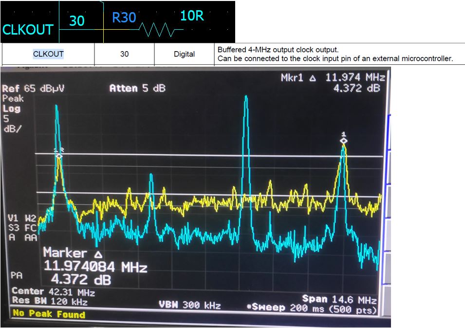
At this time, the EMC test failed. (See image below)
Currently, the CLKOUT pin of the AFE4490 is forcibly set to GND, and as a result of the operation, the data seems to be normally uploaded, but it is judged that the connection to GND should not be performed when viewing the Datasheet.

[Questions]
1) Due to an EMC problem, if the CLK OUT pin of the AFE4490 is not in a floating state, 10R on the reference circuit is not used, and is processed immediately, is there any problem with the internal circuit diagram?
2) If GND is processed after 10R on the reference circuit, is there any problem with the internal circuit diagram?
3) If there is a problem with the GND connection, is there any other way?
4) Why is the reference circuit designed in a floating state? Is it due to noise prevention? I wonder why.
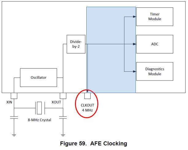
5) Is it possible to provide the internal circuit diagram of 4MHz CLK OUT? (Blue shaded part of the datasheet image below)

please check.
Thank you.