This thread has been locked.
If you have a related question, please click the "Ask a related question" button in the top right corner. The newly created question will be automatically linked to this question.
Hi,
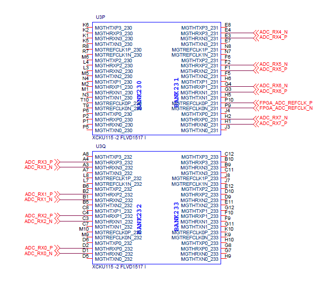
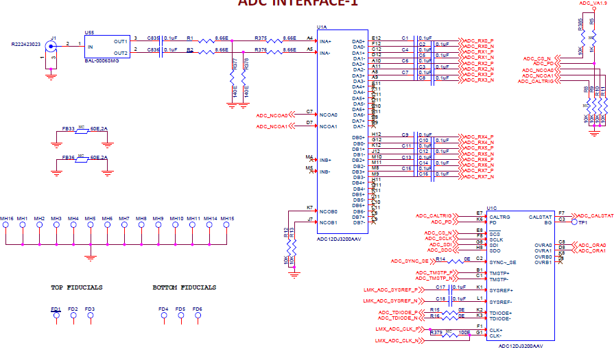
We are using ADC12DJ3200 operated in JMODE 5 for 5 GSPS. We are operating the serdes at 6.25 gbps x 8 lanes.
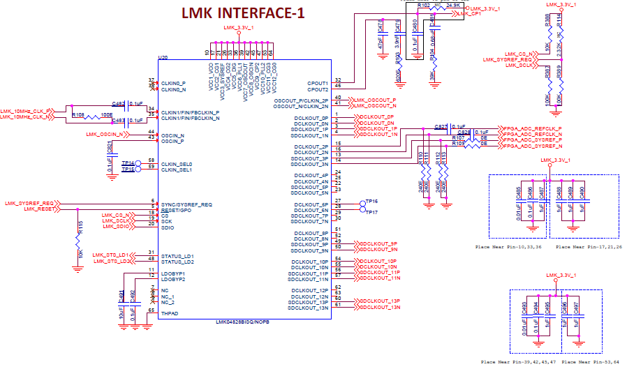
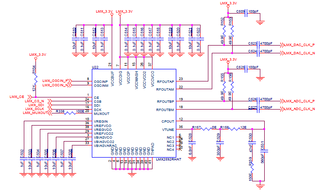
Sysref (19.53125 MHz) and dclk (156.25 MHz) for FPGA generated from LMK04828 and ADC sampling clock generated (2.5 GHz) from LMX2592.
ADC sysref also generated from LMK04828 (19.53125 MHz) for F=1 and K=32. Both FPGA and ADC are operated with same settings.
We have monitored dclk and sysref for FPGA, we are operating in LVDS and within the FPGA specs for receiving.
The sysref clock to ADC is operated with LVPECL(1600) from LMK04828, circuit to similar to ADC eval boad HSP001.
We are able to read and write the ADC. ADC debug status register reads 0x1C. ADC seems to be responding ok. But the Sync is low.
We are using PHY + JESP IP, FPGA side receives some junk data not 0xBC.
Please help, we are struck at this stage.
Regards,
Rajesh khanna
Hi Jim,
After some debugging through various posts, we found the clock from LMK is not stable. Once we made the clock stable.
We were able to pass through the JESD initialization. ADC input clock from LMX is 2.5 GHz.
Now we are finding random failure like some times JESD initialized successful, while other times it is failing.
We do following.
1. JESD RX core in reset.
2. Configure LMK.
3. Configure LMX.
4. Configure ADC.
5. Configure JESD RX core.
6. Generate Sysref
7. Release JESD Rx core reset.
8. Wait for delay (100 ms)
9. Check for status in 0x38.
If JESD link not established how do we reestablish the link.
--- ADC12DJ3200 Registers --------- Addr Rdata Name 0x000 0x0030 Configuration A Register 0x002 0x0000 Device Configuration Register 0x003 0x0003 Chip Type Register 0x004 0x0020 Chip ID Registers LSB 0x005 0x0000 Chip ID Registers MSB 0x006 0x000A Chip Version Register 0x00C 0x0051 Vendor Identification Register LSB 0x00D 0x0004 Vendor Identification Register MSB 0x010 0x0000 User SPI Configuration Register 0x029 0x0060 Clock Control Register 0 0x02A 0x0000 Clock Control Register 1 0x02C 0x0099 SYSREF Capture Position Register 0x02D 0x008D SYSREF Capture Position Register 0x02E 0x00B1 SYSREF Capture Position Register 0x030 0x00C4 INA Full Scale Range Adjust Register 0x031 0x00A4 INA Full Scale Range Adjust Register 0x032 0x00C4 INB Full Scale Range Adjust Register 0x033 0x00A4 INB Full Scale Range Adjust Register 0x038 0x0000 Internal Reference Bypass Register 0x03B 0x0000 TMSTP+/- Control Register 0x048 0x0000 Serializer Pre-Emphasis Control Register 0x060 0x0001 Input Mux Control Register 0x061 0x0001 Calibration Enable Register 0x062 0x0001 Calibration Configuration 0 Register 0x06A 0x000B Calibration Status Register 0x06B 0x0000 Calibration Pin Configuration Register 0x06C 0x0001 Calibration Software Trigger Register 0x070 0x0001 Calibration Data Enable Register 0x07A 0x00B9 Channel A Gain Trim Register 0x07B 0x00A5 Channel B Gain Trim Register 0x07C 0x000A Band-Gap Reference Trim Register 0x07E 0x009D VINA Input Resistor Trim Register 0x07F 0x00AB VINB Input Resistor Trim Register 0x080 0x00C1 Timing Adjustment for A-ADC, Single Channel Mode,FG Calibration Register 0x081 0x0080 Timing Adjustment for B-ADC, Single Channel Mode,FG Calibration Register 0x082 0x00B9 Timing Adjustment for A-ADC, Single Channel Mode,BG Calibration Register 0x083 0x00A1 Timing Adjustment for C-ADC, Single Channel Mode,BG Calibration Register 0x084 0x00E7 Timing Adjustment for C-ADC, Single Channel Mode,BG Calibration Register 0x085 0x0080 Timing Adjustment for B-ADC, Single Channel Mode,BG Calibration Register 0x086 0x0069 Timing Adjustment for A-ADC, Dual Channel Mode Register 0x087 0x009A Timing Adjustment for C-ADC acting for A-ADC, DualChannel Mode Register 0x088 0x00A4 Timing Adjustment for C-ADC acting for B-ADC, DualChannel Mode Register 0x089 0x0080 Timing Adjustment for B-ADC, Dual Channel Mode Register 0x08A 0x00A4 Offset Adjustment for A-ADC and INA Register 0x08B 0x0007 Offset Adjustment for A-ADC and INA Register 0x08C 0x000A Offset Adjustment for A-ADC and INB Register 0x08D 0x0008 Offset Adjustment for A-ADC and INB Register 0x08E 0x0000 Offset Adjustment for C-ADC and INA Register 0x08F 0x0008 Offset Adjustment for C-ADC and INA Register 0x090 0x00FB Offset Adjustment for C-ADC and INB Register 0x091 0x0007 Offset Adjustment for C-ADC and INB Register 0x092 0x006D Offset Adjustment for B-ADC and INA Register 0x093 0x0007 Offset Adjustment for B-ADC and INA Register 0x094 0x00FA Offset Adjustment for B-ADC and INB Register 0x095 0x0007 Offset Adjustment for B-ADC and INB Register 0x102 0x0064 Timing Adjustment for Bank 0 (0� Clock) Register 0x103 0x0081 Timing Adjustment for Bank 0 (-90� Clock) Register 0x112 0x0080 Timing Adjustment for Bank 1 (0� Clock) Register 0x113 0x0080 Timing Adjustment for Bank 1 (-90� Clock) Register 0x122 0x006C Timing Adjustment for Bank 2 (0� Clock) Register 0x123 0x0071 Timing Adjustment for Bank 2 (-90� Clock) Register 0x132 0x0080 Timing Adjustment for Bank 3 (0� Clock) Register 0x133 0x0080 Timing Adjustment for Bank 3 (-90� Clock) Register 0x142 0x00AF Timing Adjustment for Bank 4 (0� Clock) Register 0x143 0x0080 Timing Adjustment for Bank 4 (-90� Clock) Register 0x152 0x0080 Timing Adjustment for Bank 5 (0� Clock) Register 0x153 0x0080 Timing Adjustment for Bank 5 (-90� Clock) Register 0x160 0x0000 LSB Control Bit Output Register 0x200 0x0001 JESD204B Enable Register 0x201 0x0005 JESD204B Mode (JMODE) Register 0x202 0x001F JESD204B K Parameter Register 0x203 0x0001 JESD204B Manual SYNC Request Register 0x204 0x0002 JESD204B Control Register 0x205 0x0000 JESD204B Test Pattern Control Register 0x206 0x0000 JESD204B DID Parameter Register 0x207 0x0000 JESD204B Frame Character Register 0x208 0x001C JESD204B / System Status Register 0x209 0x0000 JESD204B Channel Power Down 0x210 0x0000 DDC Configuration Register 0x211 0x00F2 Over-range Threshold 0 Register 0x212 0x00AB Over-range Threshold 1 Register 0x213 0x0007 Over-range Configuration Register 0x214 0x0001 DDC Configuration Preset Mode Register 0x215 0x0000 DDC Configuration Preset Select Register 0x216 0x0002 Digital Channel Binding Register 0x217 0x0000 Rational NCO Reference Divisor Register 0x218 0x0000 Rational NCO Reference Divisor Register 0x219 0x0002 NCO Synchronization Register 0x297 0x0000 Spin Identification Register 0x2B0 0x0000 SYSREF Calibration Enable Register 0x2B1 0x0005 SYSREF Calibration Configuration Register 0x2B2 0x0000 SYSREF Calibration Status 0x2B3 0x0000 SYSREF Calibration Status 0x2B4 0x0001 SYSREF Calibration Status 0x2B5 0x0000 DEVCLK Aperture Delay Adjustment Register 0x2B6 0x0000 DEVCLK Aperture Delay Adjustment Register 0x2B7 0x0000 DEVCLK Aperture Delay Adjustment Register 0x2C0 0x0001 Alarm Interrupt Status Register 0x2C1 0x000D Alarm Status Register 0x2C2 0x0000 Alarm Mask Register
Regards,
Rajesh khanna.
Rajesh,
Why are reading register 0x38 for status? This is the internal reference BG_Bypass register. There is no status found here. What is the status of the SYNC? Is it toggling or stuck low? This needs to be driven low by the FPGA to start the link configuration. Try disabling the sysref receiver circuit (set address 0x29 to 0x00).
Try using the default values for the timing adjustment registers as well. Can you send your portion of the schematic that shows the ADC, LMK and LMX?
Regards,
Jim
Hi Jim,
Sorry it is 0x38 in xilinx JESD IP Register. Whereas we also read 0x208 in ADC register. In eval board we are getting 0x7C.
Occasionally our board also working, but most of the times it is struck at CGS.
Sync when not working is struck at zero and ADC jesd status(0x208) register reading 0x1C.
DCLKOUT2P/2N and SDCLKOUT3P/3N is connected to FPGA are length matched with LVDS (240 ohm is DNP).
SDCLKOUT_13P/13N is connected to ADC for sysref (240 ohm resistor with 0.1 uf series coupling capacitor, operating on LVPECL1600 from lmk)
Regards,
Rajesh khanna.
Hi Rajesh,
I would suggest you reduce the sampling clock frequency( maybe by factor of 2) and see if you are still seeing the same unstable behavior. If the system is stable as lower sampling frequency( hence lower serdes speed). It would mean data integrity issue. Also have you tried test modes on such as PRBS pattern?
Regards,
Neeraj
Hi,
I have reduced the speed and checked. We are getting same problem.
We have monitored the SERDES data from ADC we are able to see clearly the character's .
There is no degradation of the signal using high speed scope for low speed and high speed.
We also verified the device clock and sysref to FPGA which are also stable.
regards,
Rajesh khanna.
Hi Rajesh,
There is an option to use get the JESD initialization done without the syncse signal. This process is manual but should be worth a try.
1. Write the value of 0x00 to register address 0x200. This will disable the JESD block
2. Write the value of 0x0A to register address 0x204. This will ignore the status of SYNCSE pin
3. Write the value of 0x00 to register address 0x203. This will act like SYNCSE pin is pulled low and the ADC will start sending BC BC chars.
4. Reset and release the IP on the FPGA side. ( The FPGA will pull the syncse signal low and will expect the BC BC chars. Since the ADC is already sending BC chars the FPGA can lock to the it and will expect data)
5. Write the value of 0x01 to register address 0x203. This will act like SYNCSE pin is pulled high and the ADC will start sending data.
Please see if this process is working for you. If this working than I would mean either SYNCSE signal is not routed properly, SYNCSE signal is not meeting the recommended voltage level or maybe syncse signal is inverted on FPGA side.
Regards,
Neeraj