This thread has been locked.

If you have a related question, please click the "Ask a related question" button in the top right corner. The newly created question will be automatically linked to this question.

ADC10040: Single ended problem

Part Number: ADC10040

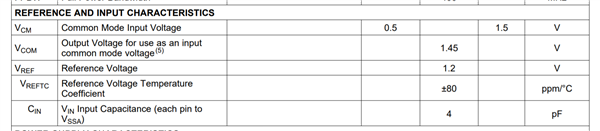
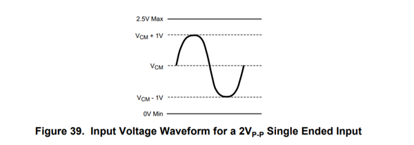
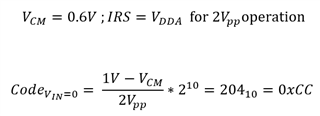
Hello, I have implemented in single ended mode the ADC10040 as described in page 20. I am observing that the digital output D0-D9 is stuck to 0 until the Vin signal reach around 350mV. Then upper 350mV, the output seems to start to decode. I have joined the VCOM to my Vin- pin as in your example.

My signal is a constant voltage for this debug. Have you any ideas because I need to sample from 0V to full scale= 2V ( IRS=1) ? Best regards

  • Hi David,

    When the output begins to decode around 350mV input, does the output start at 0 or around the expected value (~180) ?

    Regards, Chase

  • Hi Chase,

    Here is my measurement : With Vin = 500mV the output code is 0000100xxx binary so 32 decimal instead of 255 expected. I measure VREF= 1.2V VREFT= 1.99V  VrefB= 955 mV and VCOM = 1.47V . I had expected VCom to 1Volt . Have you an explanation, ?

  • Hi David,

    I've reviewed the datasheet for this device and cannot find anything wrong with your measurements. Around 1.45 is typical.

  • David,

    I have now remembered you are testing with constant voltage. VCM is the DC component of your input. Please test with a 2Vpp signal centered at 1V DC and provide your results. Despite the datasheet showing VCM as 0.5V, if you have no AC components to your input, this might cause issues as you are describing.

    Regards, Chase

  • Hi Chase, I have choosen this component to make DC measurements and not only AC measurements which would be a strong limit. On other differential inputs ADCs, the single mode is done to polarize internally the input so that the full scale of ADC is respected. Besides, the single mode schematic on page 20 is tricky and not clear at all front of what you said. As workaround, is it possible to force the VrefB voltage to 0 to direct the ADC to sample from 0V ?

  • Hi Chase,

    I will try next to add an 0.6V offset to my single ended input resulting a simple 1VDC input for example. But how the internal coding work in this case with a DC offset ?

  • Hi David,

    Of course this device can measure DC and AC, I should have said DC offset rather than DC component of input. Apologies for any confusion.

    No, it is not possible to force Vref to 0V. The datasheet states that Vref  must be 1.2V for this device. You might be able to get away with supplying lower values, but this is not stated anywhere in the datasheet so I will not recommend trying it.

    What sampling frequency is required for your application?

  • For any VCM, you will be able to capture signals between the higher of {VCM - 1V , 0V} and the lower of {VCM + 1V , 2.5V}.

    With a 0.6V offset (VCM = 0.6V), you will be able to capture between 0V and 1.6V.

  • Hi Chase, my sampling frequency is currently 24 MHz. I have talked about VrefBottom and not Vref as there is a current source within the first stage.  Whatever the case, at which voltage is the code 0x0 in single ended ? what is the formula knowing that DF pin is in offset binary ?

  • David,

    I am not sure at which voltage will produce the code 0x0 offset binary. For cases of 2Vpp operation and VCM less than 1V, I imagine it is not possible to for code 0x0 as an output. For this case, I would recommend counting from the max downward.

    For example, with VCM of 0.6V, the output code for 0V on the input will be 0xCC. I've found this by using the following (which should apply for all cases where VCM is less than or equal to 1V.) Does this answer your question?

    Regards, Chase

  • Hi Chase,

    Sorry but it is not clear for me. May you ask the design team the real formula for this single ended mode for all Vin. For me, Vin must be soustracted to a threshold to know. Vcm is virtual common mode and Vcom = 1.47V . Vcom appears to be the middle of VrefT and VrefB. May you ask the formula , please ?

    Best regards.

  • Hi Chase,

    After adding an offset on my single ended input (Vin+), I have done some measurements with an external power supply on Vin+ with constant values.

    Besides, I have reflect on the possible ADC internal architecture and the conclusion is that the formula is the following and it works very well:

    ADC value = [( Vin+ - VCOM) - (-1V)] *1024/2     ( with IRS pin = 1 meaning 2Vpp) to be simplified by:

    ADC value = ( Vin+ - 0.47)*1024/2

    It would be fine that you confirm it by modifying the datasheet because it's not obvious and 50% of

    customers could use the single ended mode. It's work fine with condition to have a VCM > 0.5V.

    For my board , I have set a VCM to 0.6V to have a small margin.

    Have I gain a gift for this support ? :)

    Best regards.

  • Hi David,

    I'm glad you were able to resolve your question on your own. I will pass the info on. Unfortunately, there is no gift for doing so Smiley

    Regards, Chase