This thread has been locked.

If you have a related question, please click the "Ask a related question" button in the top right corner. The newly created question will be automatically linked to this question.

SNR data required for the ADC ADC16DV160 at 1100MHz

Other Parts Discussed in Thread: ADC16DV160, ADC16V130, LMX2581, LMX2541

We are looking for an ADC for our RF signal 1100MHz (under sampling) for the data bandwidth of 20MHz.

We need the following specifications for ADC to do under sampling,

1. FPBW  >= 1100MHz

2. Sampling >= 150MHz

3. Resolution = 14bit or above

4. SNR at 1100MHz >=60dB @150MSPS sampling

5. Power dissipation < 1.5W


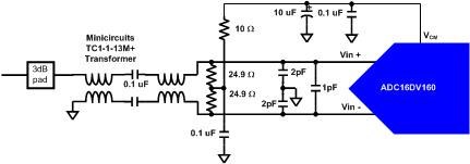
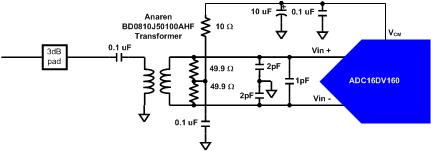
For the above requirement we have checked your ADC : ADC16DV160 which meets the all the requirement. But we are unable to find the SNR Value for our Frequency of 1100MHz from your datasheet. (SNR data available upto 200MHz input frequency)


Kindly share the SNR data at 1100MHz to proceed us further. We are looking or an SNR >=60dB at our 1100MHz frequency.

Note: We will put one more channel in idle mode.

Regards,

Sugumar K

India.

  • Hi Sugumar


    At high input frequencies, the SNR is dominated by the sample instant jitter. The total additive jitter of the ADC16DV160 is approximately 80fs. Therefore to achieve 60 dB SNR at 1100 MHz the clock jitter must be limited to around 126fs rms. As long as the clock source jitter is lower than this figure then 60dB is achievable.


    The table below shows estimated SNR for 1100 MHz Fin at -1dB input level for different amounts of clock jitter.


    SNR [dBFS]@-1dBFS input level

    Total rms Jitter [fS]

    Clock source rms jitter [fS]

    65.81

    80

    0

    63.99

    100

    60.00

    62.13

    125

    96.05

    60.59

    150

    126.89

    59.28

    175

    155.64

     Best regards,

    Jim B

  • Hi Jim,


         Thanks for your SNR vs jitter data at 1100MHz.

    1) Do you have any recommended circuit (clock source / Jitter cleaner) to achieve <150fs Clock source jitter to achieve the SNR around 60dB by using your ADC part ADC16DV160?

    2) Also we need to know , Whether your single channel ADC: ADC16V130 (130MSPS) also will give the same SNR performance for the above mentioned clock jitter values?


    Regards,

    Sugumar K

  • Hi Sugumar

    1) For a low jitter clock source in the 130 to 160 MHz frequency range I would recommend either the LMX2581 or LMX2541.

    2) Since the additive jitter of the ADC16V130 is the same as that of the ADC16DV160 (80fs) the SNR calculations at 1100MHz input frequency will be the same.

    Best regards,

    Jim B


  • Hi Jim,


        We are planning to use your ADC ADC16DV160 for under sample our RF signal 1100MHz at 160MSPS.


    In the above table you have mentioned that the ADC SNR [dBFS] is 60.59dB for Clock Total rms Jitter [fS] of 150fs @-1dBFS input level. It is ok for us.


    Also we have one more question, when we apply low input signal around -65dBFS then the clock jitter impact will be very less even though at our frequency of 1100MHz.

    May I know the ADC SNR value at the below input power levels while under sampling our RF signal 1100MHz at 160MSPS.


    Input Signal level     ADC SNR

    -65dBFS                      ????

    -70dBFS                      ????

    -75dBFS                      ????

    Regards,

    Sugumar K

  • Hi Sugumar

    Many of us are out of office for the US Thanksgiving holiday returning on Nov 30th.

    The earliest I may be able to look into these estimates is Saturday Nov. 28.

    Best regards,

    Jim B

  • Sugumar,

    The SNR performance at the amplitudes you are curious about (-65dBFS and below) are so low that the SNR performance will be very close to the base SNR of the device with no jitter impact, 78dBFS.

    Regards, Josh
  • We are planning to ADC part ADC16DV160 at 1100MHz signal for the full scale signal of +10dBm (50Ohm) in normal operation.

    We are planning to use your recommended circuit as per you datasheet (Figure 29) at Page No: 18. It is mentioned in the Absolute Maximum Ratings of Voltage at CLK, Vin Pins -0.3V to (VA1.8+0.3V) and mentioned (Not to exceed 2.35V).


    1. Now what should be the maximum RF input in dBm level to this ADC input transformer?


    2. The maximum voltage 2.35V mentioned is with respect to GND or common mode voltage?


    Request you to explain the same with maximum input level to the ADC for our operation.


    Regards,

    Sugumar K

  • Sugumar,

    Per the Input Clock Amplitude values in electrical tables of the datasheet, the max input swing is 3.7Vpp-diff centered about the common mode (internally biased). The ADC clock input is high impedance, so converting this voltage to a power number requires an external termination. If you use a 100 ohm differential termination at the ADC input like the EVM, then the power of 3.4Vpp-diff would be P = 10log((3.4/2)^2/2*1000/100) = 11.6dBm. The transformer has about 0.5dB insertion loss, so the input to the transformer should be 12.1dBm maximum.

    The absmax rating for the CLK input pins is relative to GND.

    Regards, Josh

  • Hi,

         We need to calculate the Cascaded noise figure with our RF Receiver module and ADC to estimate the system Noise figure. For that kindly provide the ADC ADC16DV160 noise figure (dB) or Noise-Spectral-Density (dBFS/Hz) to proceed us further.


    Our RF Frequency is 1100MHz and sampling is 160MSPS for your reference.

    Regards,

    Sugumar K

  • Sugumar,

    The input full scale range of the ADC16DV160 for a full scale 2.4Vpp sinusoid, and assuming a 100 ohm differential termination at the ADC input is, FScale = 10*log10((2.4/2)^2/2*1000/100) = +8.6 dBm. The small signal SNR = 78 dBFS and the sampling rate is 160MSPS. This leads to a noise spectral density (in dBm/Hz units) of

    NSD = FScale - SNR - 10*log10(Fs/2) = +8.6 - 78 - 10log10(160e6/2) = -148.4 dBm/Hz

    The NF at room temp can then be calculated as

    NF = -148.4 - (-174) = 25.6 dB

    Note that for larger input signals conditions, the NSD and NF will be degraded by clock jitter. This can be accounted for by adjusting the SNR value in the NSD equation.

    Regards, Josh

  • Hi Josh,


        We are planning to use ADC16DV160 ADC input as 50Ohm for the full-scale of 2.0Vp-p configuration which is corresponds to +10dBm RF input power.

    NSD = FScale - SNR - 10*log10(Fs/2) = +10 - 78 - 10log10(160e6/2) = --147.0 dBm/Hz

    The NF at room temp can then be calculated as

    NF = -147.0 - (-174) = 27.0 dB


    As per the above configuration we are planning to proceed to work and we will verify our cascaded noise figure for our system.


    Is there any issue in this above configuration?


    Regards,

    Sugumar K

  • Calculation looks good

    Cheers, Josh

  • We are planning to use the ADC input as 50Ohm differential to operate maximum input power of +10dBm for corresponding 2Vp-p.
    So kindly suggest a application circuit with ADC input components for our operating frequency of 1100MHz for 50Ohm differential input load at ADC.

    Also request you to suggest a low jitter clock source application circuit/ parts for our sampling frequency of 160MHz for better ADC SNR performance at our operating frequencies of 1100MHz.

    Regards,
    Sugumar K
  • Can we use the Mini-circuits 1:1 Balun transformer TC1-1-13M+ at ADC input for our high frequency RF input signal of 1100MHz sampling at 160MSPS.

    Also Request you to provide the application circuit for the same for 50Ohm ADC input impedance to meet the maximum input power of +10dBm.
  • Sugumar,

    Yes, you can use the TC1-1-13M+, or the MABA-007159 (similar device from MA/COM). They will both yield similar performance. Anaren's BD0810J50100AHF looks like it might do very well as well. You can do something like one of the circuits below.

    There will be a trade-off between dynamic distortion performance (H2, H3) and Input bandwidth which depends on how you set the value of the capacitors at the input of the ADC. They are meant to provide charge to dissipate the ADC's charge kickback, but they do limit the bandwidth. I think you must experiment to find the optimal tradeoff point.

    Our LMK (LMK040xx, LMK0480x) clocking products are a good match-up with this device. 

    Regards, Josh

  • Hi,

    As you said above without any jitters the SNR very close to the base SNR of the device 78dBFS. But we are doing ADC sampling at 160MSPS whereas our data bandwidth is only 16MHz. As per the FFT process gain, 10×log(Fs/(2XBW)) expecting additional processing gain of 7dB. So the final ADC SNR value expected is = 78dB (SNR) + 7dB (processing gain) = 85dB SNR.
    But we need to know whether we are able to see this SNR before DDC in FPGA or in the RAW ADC output itself?

    Regards,
    Sugumar K
  • Sugumar,
    When you observe the data at the output of the ADC, you will observe the signal plus the base thermal noise (limits base ADC SNR to 78dBFS) plus noise due to clock jitter. Processing gain occurs during filtering which occurs in your DDC. Therefore, your signal path will not have SNR=85dB until after the DDC.

    If you are just analyzing noise performance of the ADC and want to include processing gain, then you can take the ADC output data, calculate the FFT, and then do a power ratio calculation using only the spectrum band of interest.

    Regards, Josh