This thread has been locked.

If you have a related question, please click the "Ask a related question" button in the top right corner. The newly created question will be automatically linked to this question.

ADS7947 Power-up sequence

Other Parts Discussed in Thread: ADS7947

Hi,

The behavior of the ADS7947 is not as expected in our custom board.

【Question】

 Is there any prescriptions for up sequences at power on to the voltage applied to the AVDD pin and DVDD pin and REF pin?

【Issue】

   CS and SCLK are sent, but SDO data are not outputted.

 When the AVDD launch slower than DVDD, it works fine.

【Settings】

  AVDD=5V、DVDD=3.3V、REF=5V
  PDEN=0V、
  CS…pullup to 3.3V at startup
  CHSEL…Hi-Z at start up,ch will be changed 1 second later of a startup.
  Insert a 4.7μF capacitor between REF and REFGND

Best regards,
Seishin

  • Hi Seishin,

    To the best of my knowledge there is no special sequence to power up required.  The standard requirements per the Absolute Maximum RatingsTable is that the digital signals must remain low prior DVDD starting up; and the analog inputs and REF pin should not exceed AVDD during the sequence.  The digital supply voltage range is 1.65<DVDD < AVDD; therefore the DVDD voltage is to be kept below AVDD.

    Is the REF voltage or AINxP voltage high prior AVDD powering up? Are the SCLK, PDEN digital inputs low pior DVDD powering up? Is it possilbe to keep CH SEL low prior power up?  What is the AVDD/DVDD ramp rate and delay between the supplies ramping up when the issue occurs?  

    If possible, please post an oscilloscope plot showing AVDD, DVDD, REF power up sequence when the issue occurs (and also when AVDD is slower when the issue does not occur). 

    Thanks and Regards,

    Luis

  • Hi Luis,

    Sorry for not replying sooner.

    Is the REF voltage or AINxP voltage high prior AVDD powering up?

     → REF voltage or AIN voltage is lower than the AVDD prior AVDD Powering up.

    Are the SCLK, PDEN digital inputs low pior DVDD powering up?

    → SCLK,PDEN digital inputs are low prior powering up.

    Is it possilbe to keep CH SEL low prior power up?

    → It was the same result even if continued to the CH SEL low prior power up.

    What is the AVDD/DVDD ramp rate and delay between the supplies ramping up when the issue occurs?

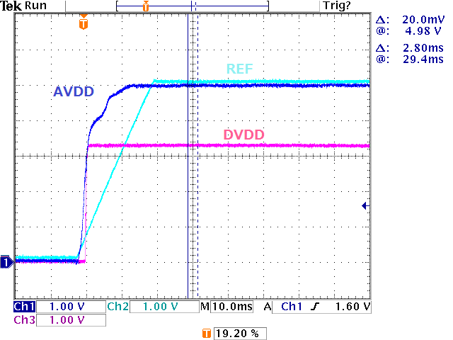
    → Please see attached photo.

    <Oscilloscope plot>

    Power-up sequence waveform when the issue occurred.

    It is the same waveform even when the issue does not occur.

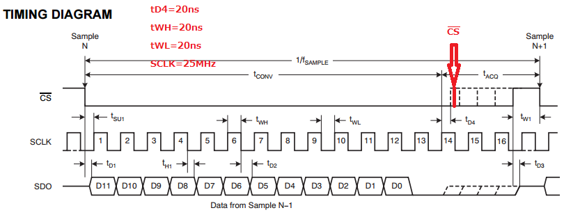
    There is a point to be worried about in the timing of the interface logic.

    When the 14th falling edge of SCLK and the CS riging edge are the same,there is no output from the SDO.

    It was found that the SDO is not output despite meets the timing requirements.(tD4: MIN 10ns)

    SDO may be output by a change of the skew when I touch it with a finger.

    Are there any timing requirements about the interface logic that are not listed on the data sheet?


    Best regards,
    Seishin

  • Hi Seishin,

    Is it possible to obtain a couple of oscilloscope plots of SCLK, CS, SDO when CS rising edge is the same as the 14th SCLK falling edge when the issue occurs?

    Please ensure to place the oscilloscope probes right at the SCLK, SDO, CS GND pins of the device. 

    I will also test the interface timing conditions used on your setup.  Please allow a couple of days.

    Thanks and Best Regards,

    Luis

  • Hi Seishin,

    One possibility is that the device may be somehow powering up on 32-CLK mode. It may be possible that this could occur under certain conditions.

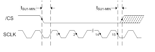
    In order to change from 32-clock mode to 16-clock mode, 15 falling clock edges must be sent to the ADS7947 while chip-select is low. To assure that the15th falling clock edge is properly received by the ADS7947, chip-select must stay low for at least 3.5ns after the 15th falling clock edge. This chip-select delay corresponds to the minimum tSU1 specification.  Please see plot below for the frame required to return to 16-CLK mode:

    Once the device is set to 16-CLK mode, the subsequent frames only require CS to be low for 10ns longer than the 14 SCLK falling edge as you have previously mentioned. Please let me know if using a 15 SCLK falling edges during the first frame, and 14SCLK falling edges for the second and subsequent frames works in the system.

    Thank you,

    Luis   

  • Hi Luis,

    Thank you for your input on this matter.

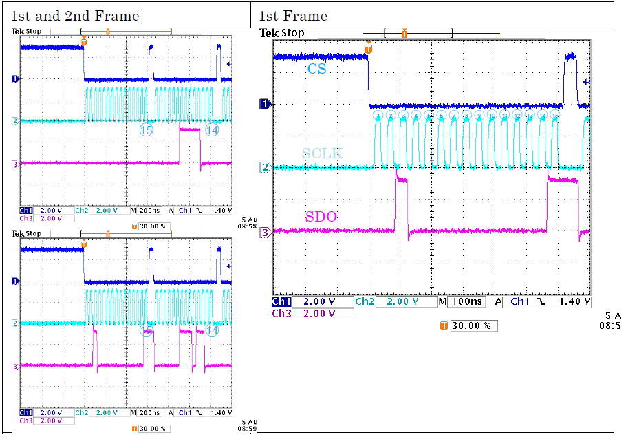
    The Oscilloscope waveform is attached.

    Oscilloscope plots_ADS7947_Seishin.xlsx

    Please let me know if you find anything wrong.


    Best regards,
    Seishin

  • Hi Seishin,

    I don't see anything wrong with the interface timing.  One possibility is that the device is somehow powering up on 32-CLK mode due to some power-up supply rate/sequence sensitivity occuring in the system.  If the device is starting up in 32-CLK mode, this would explain why no data data is available on SDO when using 14-CLK frames.  One way to guarantee that the device is set to 16 clk mode after power-up, is to always use 15 falling clock edges on the first frame immediately after power-up.  After the first 15-CLK frame is issued,  a 14 CLK frame may be used for the second and subsequent frames.  Please see below description to change from 32-CLK frame to 16-CLK frame.

    In order to change from 32-clock mode to 16-clock mode, 15 falling clock edges must be sent to the ADS7947 while chip-select is low. To assure that the15th falling clock edge is properly received by the ADS7947, chip-select must stay low for at least 3.5ns after the 15th falling clock edge. This chip-select delay corresponds to the minimum tSU1specification.  Once the device is set to 16-CLK mode, the subsequent frames only require CS to be low for 10ns longer than the 14 SCLK falling edge.

    Please let me know if using a 15 SCLK falling edges for the first frame after power-up, and 14SCLK falling edges for the second and subsequent frames works in the system.

    Thank you and Best Regards,

    Luis

  • Hi Luis,

    The issue was solved.

    I am very grateful for your cooperation.

    By using the 15SCLK falling edge for the first frame after power-up,SDO was normally output.(See below)


    Please let me confirm one last thing.

    You may need to 15SCLK falling edge in order to change to the 16-clock mode,

    please tell me where that is mentioned in the datasheet.

    Thanks and best regards,

    Seishin

  • Hi Seishin,

    I am glad that the issue was resolved.  Unfortunately, the procedure to return to change from 32 -clk mode to 16-clk is currently not mentioned, but will be noted in the next datasheet revision; I have provided the feedback. 

    Please let me know if you require anything.   

    Thank you and Kind Regards,

    Luis