This thread has been locked.

If you have a related question, please click the "Ask a related question" button in the top right corner. The newly created question will be automatically linked to this question.

ADS8691: Abnormal output of converted value when inputting sine wave voltage of about 1.6V or more.

Part Number: ADS8691
Other Parts Discussed in Thread: OPA141,

Dear All, 

My last problem was solved with your help. Thanks again.

When the ADC input test was performed based on the completed code, it was found that the converted value was abnormal when a sinusoidal voltage signal having a specific voltage (about 1.6 V) or more was input.

However, it does a stable and accurate conversion for input signals below 1.0V.


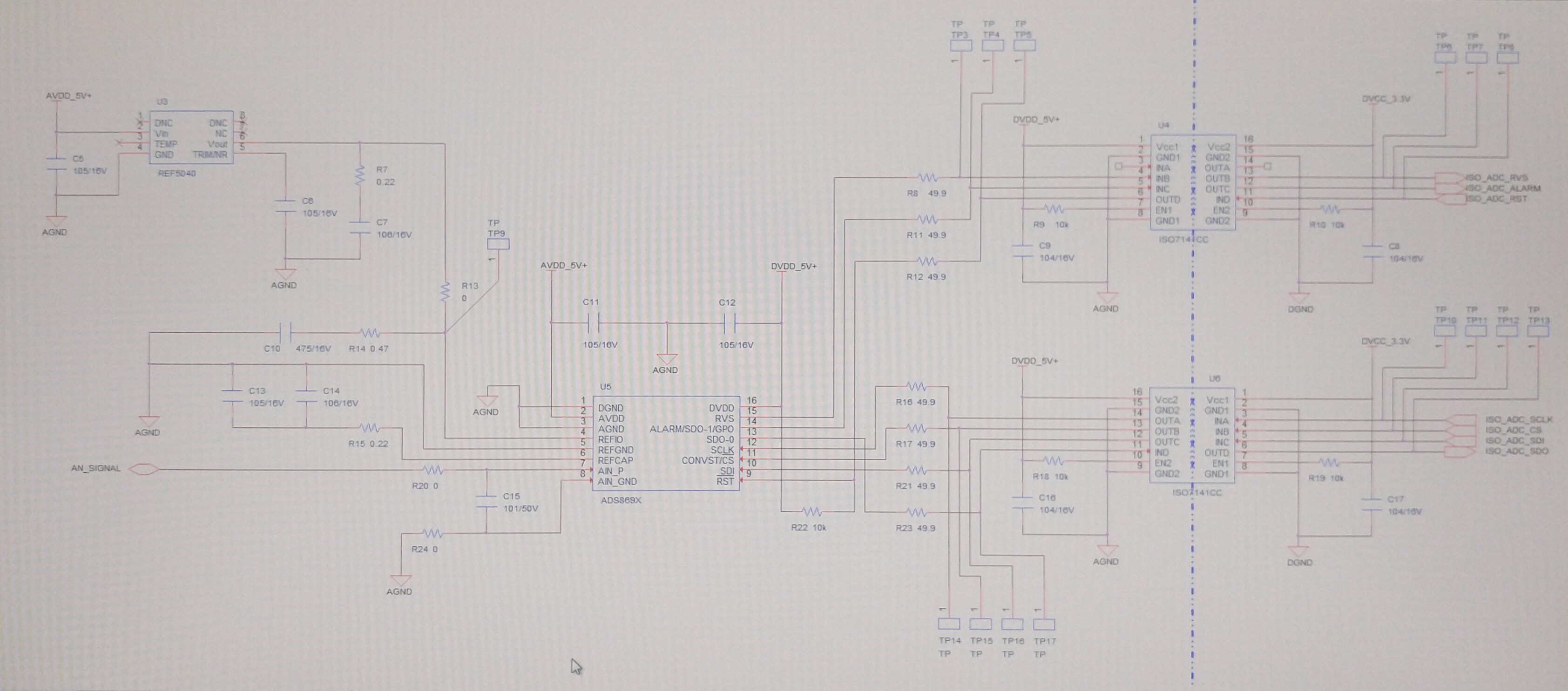
The operating conditions of my ADC are as follows.

Input Range of ADC: ± 5.12V
Signal source: function generator (output impedance: 5 ohms)
Signal source and ADC side element: 5Hz 2nd-order HPF with OPA141
Sampling: 4096 at a rate of 16,384 per second, collected for 250 msec.

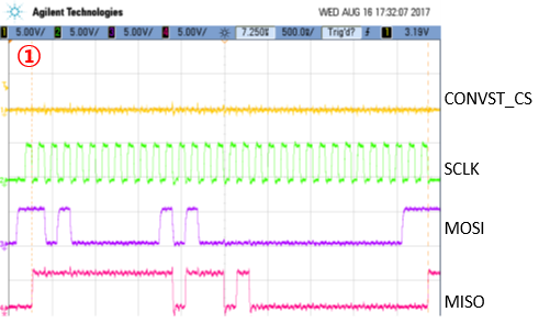
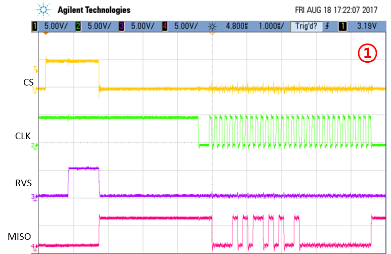
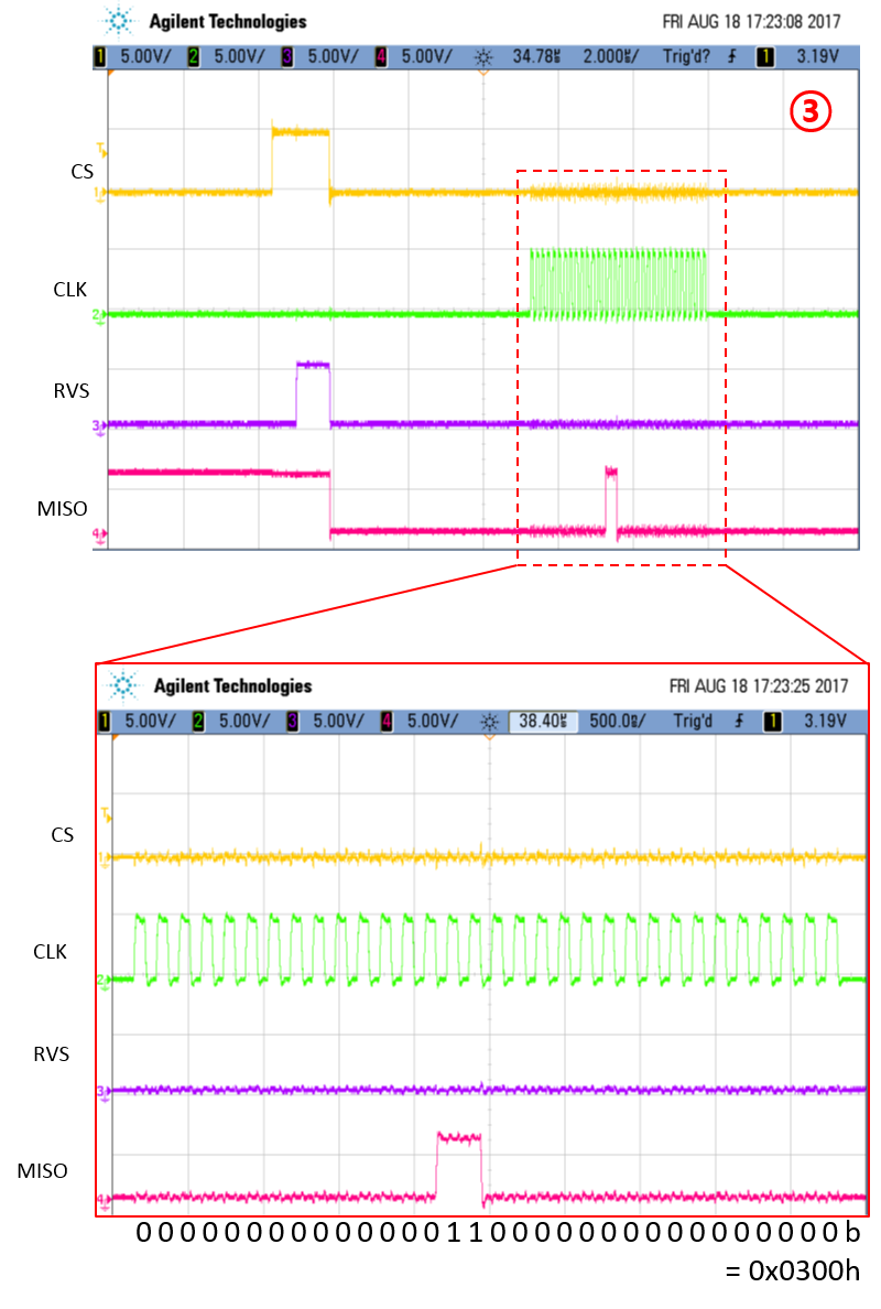
The converted value does not match the set input range and periodically outputs a value of 0.

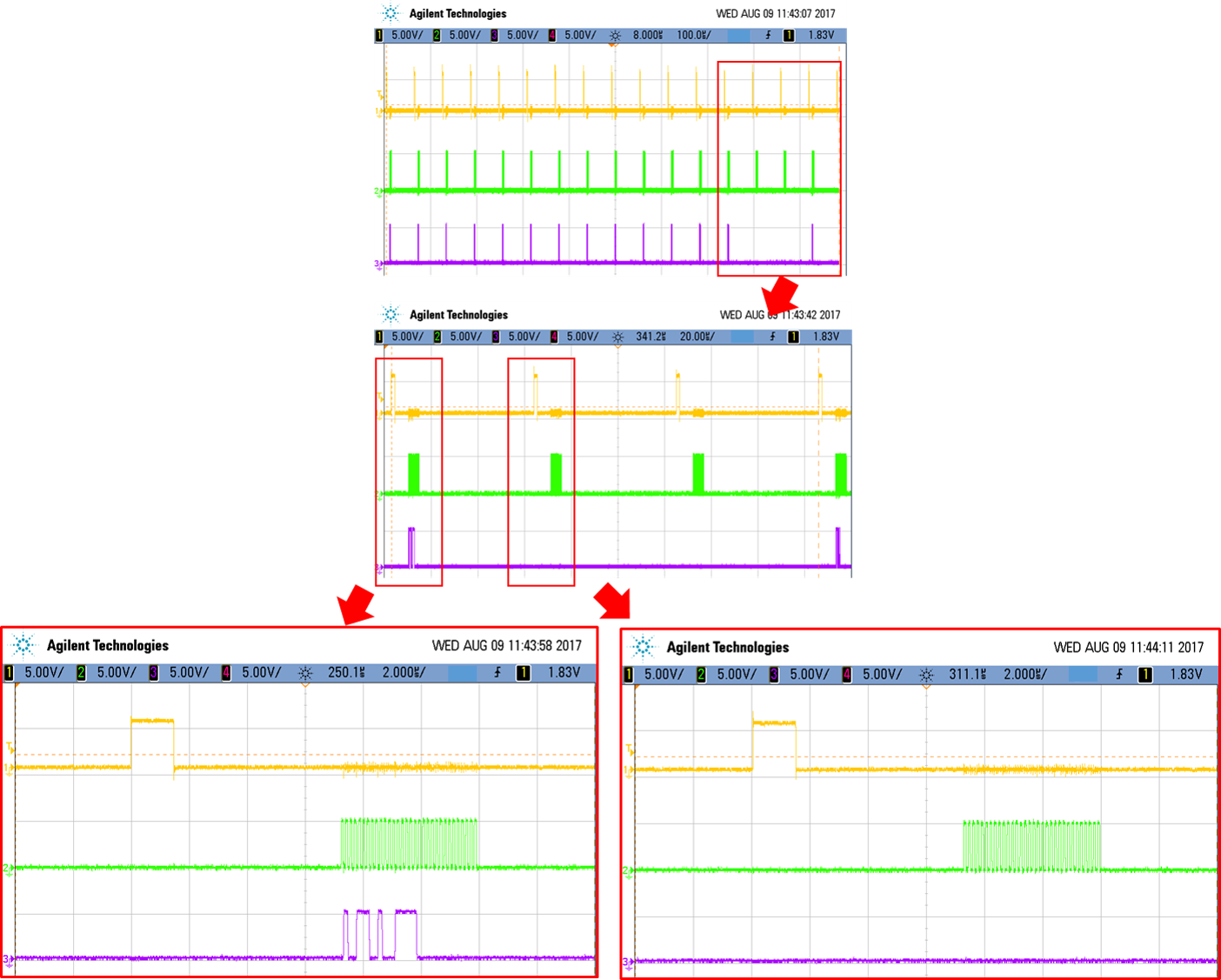
Analysis of the oscilloscope waveform shows that zero MISO signal is output from the ADC.

In these symptoms, are there any cases that can be classified as probable problems or potential failures?

  • Hi Young-Kyo,

    I will look into this. Would you be able to share your schematic?

    -Cynthia
  • Dear Cynthia, 

    Here is a schematic of the ADC part. 

    Note that R13 is not currently inserted.

    Would you please give me your email address? If you let me know, I can provide more information.

  • thanks Young-Kyo,

    Your schematic looks good, I can simulate it using TINA to confirm that the circuit works well. I will need your inpur signal frequency to do this though.

    The most likely culprite is the digital isolators, they introduce a propagation delay that could be disrupting your ADC digital readings.
    Below are two good TIDesign that explains how to use isolators and mitigate their effects.

    http://www.ti.com/lit/ug/tiducm8a/tiducm8a.pdf

    http://www.ti.com/lit/ug/tidubj1/tidubj1.pdf

    Regards

    Cynthia

  • Thanks Cynthia,

    Based on your advice, we assume the cause of this problem as an isolator and remove it.

    After removal, I connected directly to the wire as shown in the picture below.


    However, the issue raised above was still repeated.

    As a result of careful observation, the problem was repeated in the signal conversion of about 2.0 V (almost 1.93 V) or more, and it was operated normally at the signal below that.

    Sometimes, when inputting a signal of 2.0V or more, the peak value of the conversion result was expressed same the input voltage, but there still occurred an interval in which there is no MISO signal of the SPI.

    In additional observations, the peak value of the conversion result does not exceed 2.0 V even if a signal of any level above 2.0 V is input. Also the ADC's MISO signal is still periodically zero.

    Is there another possible cause of this problem?

    I think the problem of the reset procedure of the ADC or the length of the CONVST signal is another cause of the problem, but it is not clear.

    Regards

    Young-Kyo

  • Dear Cynthia,


    I have solved this problem now, but I wonder if my solution is reasonable.


    The abnormal data output phenomenon of ADS8691 that occurred to me (periodic MISO signal becomes 0 when data conversion over 2V) was not solved by hardware modification.
    but, I solved the problem by modifying the ADC's operating sequence at the firmware level.

    Previously, after the MCU was powered up, the register values for the ADC's Input Range (0x14h, 0x0003, ± 5.12V range) settings were written once before entering the loop.

    Then, the converted value is read periodically through the SPI communication within the timer interrupt for signal sampling. (sampling rate is 16,384 sample per second)

    The above flow of the code returned the ADC converted value normally at input signal below 2.0V, but the MISO signal periodically returns 0 for the above voltage signal, or normal ADC conversion could not be performed.


    As a workaround, I moved register write code for the ADC Input Range (0x14h, 0x0003, ± 5.12V range) to inside the timer interrupt.

    Immediately thereafter, the code that reads the ADC conversion value is placed.

    In other words, the register write code for the ADC Input Range that was executed only once is now run each sampling period in timer interrupt.

    The modified code configuration now gives me the normal ADC conversion value.


    I wonder if this modified code flow is a reasonable code structure.

    It can be understood that a typical ADC operation is a repetitive read operation after a single register setting in the ADC initialization routine.

    However, in this modified code that leads to normal operation, the register write operation and the ADC value read operation are repeated in a single set.

    I think that the register write operation through the unnecessary SPI communication inside the interrupt routine is unreasonable in terms of MCU resource management.

    In order to get the periodically converted value for the operation of the ADS8691, does the write operation necessarily come before the SPI read operation?

    I need the opinions of your experts.


    Regards
    Young-Kyo.
  • Young-Kyo

    That is interesting, since you were able to get the correct readings with your work around, that rules out that there is a hardware issue, and leaves the software programming as the culprit of the problem.
    Would you be able to read the register content after just one time through the loop after seeing the reading issue. I would like to confirm that the registers are programmed correctly, and remain programed. If not, this could explain why reprograming it through the loop every time the device functions correctly.

    Thanks
    Cynthia
  • Dear Cynthia

    The code below is the code I tested, which is the one that writes and reads the register before it enters the loop.

    I also added a screenshot of its oscilloscope beneath that code.

    //=====================================================================================//

    define CLEAR_HWORD 0x6000
    #define READ_HWORD 0xC800
    #define READ                 0x4800
    #define WRITE               0xD000
    #define WRITE_MS       0xD200
    #define WRITE_LS        0xD400
    #define SET_HWORD   0xD800

    #define DEVICE_ID_REG          0x02 // Device ID register
    #define RST_PWRCTL_REG     0x04 // Reset and power control register
    #define SDI_CTL_REG              0x08 // SDI data input control register
    #define SDO_CTL_REG            0x0C // SDO-x data input control register
    #define DATAOUT_CTL_REG   0x10 // Output data control register
    #define RANGE_SEL_REG       0x14 // Input range selection control register
    #define ALARM_REG                0x20 // ALARM output register
    #define ALARM_H_TH_REG    0x24 // ALARM high threshold and hysteresis register
    #define ALARM_L_TH_REG    0x28 // ALARM low threshold register

    uint16_t ADC_Command = 0;
    uint32_t ADC_Result = 0;
    extern uint8_t TIM7_Flag;
    uint8_t SPI1_ADC_RxBuffer[8] = {0};
    uint8_t SPI1_ADC_TxBuffer[8] = {0};

    /* Private function prototypes -----------------------------------------------*/
    void SystemClock_Config(void);
    static void MX_NVIC_Init(void);

    int main(void)
    {

    /* MCU Configuration----------------------------------------------------------*/

    /* Reset of all peripherals, Initializes the Flash interface and the Systick. */
    HAL_Init();

    /* USER CODE BEGIN Init */

    /* USER CODE END Init */

    /* Configure the system clock */
    SystemClock_Config();

    /* USER CODE BEGIN SysInit */

    /* USER CODE END SysInit */

    /* Initialize all configured peripherals */
    MX_GPIO_Init();

    HAL_GPIO_WritePin(GPIOA, GPIO_PIN_4, GPIO_PIN_RESET); // SPI1_NSS pin go to LOW
    HAL_GPIO_WritePin(GPIOA, GPIO_PIN_5, GPIO_PIN_RESET); // SPI1_SCK pin go to LOW
    HAL_GPIO_WritePin(ADC_RST_GPIO_Port, ADC_RST_Pin, GPIO_PIN_RESET); // ADC RESET
    HAL_Delay(100);
    HAL_GPIO_WritePin(ADC_RST_GPIO_Port, ADC_RST_Pin, GPIO_PIN_SET);

    MX_DMA_Init();
    MX_SPI1_Init(); // SPI_CS Control by Hardware
    MX_SPI4_Init();
    MX_TIM6_Init();
    MX_TIM7_Init();
    MX_USART1_UART_Init();

    /* Initialize interrupts */
    MX_NVIC_Init();

    HAL_TIM_Base_Start_IT(&htim7); // For ADC Sampling

    /* USER CODE BEGIN 2 */

    ////// Set ADC Input Range with Internal Refrence Enable

    ADC_CONVST_CS();

    ADC_Command = WRITE + RANGE_SEL_REG;
    SPI1_ADC_TxBuffer[0] = (uint8_t)(ADC_Command >> 8);
    SPI1_ADC_TxBuffer[1] = (uint8_t)ADC_Command;
    SPI1_ADC_TxBuffer[2] = 0x00;
    SPI1_ADC_TxBuffer[3] = 0x03; // ±1.25V * Vref and Internal Refrence Enable

    HAL_SPI_Transmit_DMA(&hspi1, SPI1_ADC_TxBuffer, 4);
    while( hspi1.State == HAL_SPI_STATE_BUSY_TX );

    ADC_CONVST_CS();

    // ------------------------------------------------------- //

    ////// Send read command for RANGE_SEL_REG

    ADC_CONVST_CS();

    ADC_Command = READ_HWORD + RANGE_SEL_REG
    SPI1_ADC_TxBuffer[0] = (uint8_t)(ADC_Command >> 8);
    SPI1_ADC_TxBuffer[1] = (uint8_t)ADC_Command;
    SPI1_ADC_TxBuffer[2] = 0x00
    SPI1_ADC_TxBuffer[3] = 0x00

    HAL_SPI_Transmit_DMA(&hspi1, SPI1_ADC_TxBuffer, 4); // Send Read half word Command
    while(hspi1.State == HAL_SPI_STATE_BUSY_TX); // Wait for Transfer complete.

    ADC_CONVST_CS();

    // ------------------------------------------------------- //

    ////// Read from SPI frame (F+1)
    ADC_CONVST_CS();

    HAL_SPI_Recevie_DMA(&hspi1, SPI1_ADC_RxBuffer, 4); // SPI Recevie
    while(hspi1.State == HAL_SPI_STATE_BUSY_RX); // Wait for Recevie complete.

    ADC_CONVST_CS();


    //======================================================================//

    // User code.......//


    while(1) {}

    }

    //=====================================================================//

    ① : Set ADC Input Range with Internal Refrence Enable

    ② :  Send read command for RANGE_SEL_REG

    ③ : Read from SPI frame (F+1)

    My suspicion is that SCLK is input to the ADC after the first part of SCLK changes from high to low.

    Please check whether the flow of this code and the signal output according to it is normal and Please let us know your opinion.

    Regards

    Young-Kyo.

  • Hello Young-Kyo

    Would you eliminate the double pulse for CS?
    You could be reading while the device is still converting. To see if this is happening, also probe RVS and be sure that you are not reading while RVS is still showing its converting. Every time a CS pulse is sent, the device begins a new conversation, thus with the double pulses, you could not be giving the device enough time to finish the conversions before reading.


    -Regards, Cynthia

  • Hello Cynthia, 

    Based on your advice, I removed the double CS from the previous code.


    In addition, the RVS signal was examined through an oscilloscope.


    It seems to be normal activate with after tconv_max.


    However, the abnormal output of the ADC conversion result is still continuing.


    During I looked closely at the oscilloscope waveform, I found one strange thing.

     
    In the write operation of the ADC's input range register, the value of 0x0003 is transmitted when the register value is transmitted to the 14h address of the ADC. (See the code in the previous post)

    But, the value output from the 14h address in the read operation of the ADC's input range register is 0x30000. (See image above screenshot)

    Does a byte swap occur while receiving data from the ADC?
    I wonder if these results I obtained are normal.

    Regards. 

    Young-Kyo.

  • Young-Kyo

    This device does not have a byte swap. The last screenshot is showing the correct information. The SDO  (MISO) data reads 00030000.

    The code shows that you wrote x00h followed by x03h.  That would have 12 leading zeros, and a 3h. The device then adds 16 lagging 0 to fill the 32 bits. The screen shows that the register is being written to correctly and reading out the correct information as well. In the page 42 of the datasheet, it is further explained.

    I'm looking into replicating your issue. thus far it looks as you are setting up the device correctly. I believe when the device sees a sudden change in range, it is being reset inadvertly, probably somehwere further in the code. As you had menitoned before this would deal with the reset procedure of the ADC or the length of CS (if CS is held high at the end of a conversion, the device enters NAP mode, this would need to be enabled as the default is this mode not active).

    Regards,

    Cynthia