This thread has been locked.

If you have a related question, please click the "Ask a related question" button in the top right corner. The newly created question will be automatically linked to this question.

DAC7760: What is the damage reason of DAC7760 ?

Part Number: DAC7760

dear sir


We control the DAC7760 output voltage or current through the SPI interface, and then measure the voltage or current using a multimeter, directly connected to the connector.
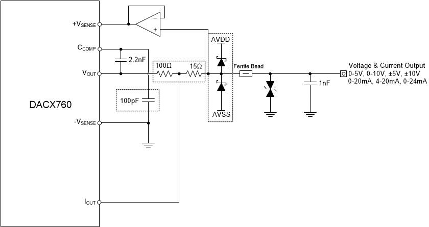
In this processwe found short circuit between the power supply of DAC chip and GND,there is a R3 between AVDD and Boost, we put a 15 ohms  in the output current to

limit the current , but when IOUT  connect to GND, the DAC7760  damage, do we have a short circuit protection ? what`s the  proper load resistance ?

  • Du,

    Can you please elaborate further on the conditions and outcome of your tests?

    Specifically:

    - Which output is active during your tests? VOUT or IOUT? Either?
    - Can you share any details concerning the parameters of the clamp diodes?
    - Similarly, can you provide the details for the TVS diode? I cannot reliably read the part number
    - Are you performing tests while the VOUT or IOUT are active?
  • Dear duke

    Place DAC7760 in current mode, output 19mA, open circuit.
    At this time, short connection and disconnection of output and GND for several times will immediately damage DAC, In our actual use, when used for a long time, it is very likely to occur Iout short connector, resulting in similar damage.
    Is such damage characteristic of the chip itself?Or do we have design flaws?Is there any way to prevent such damage? how to set the proper output limit resistance ?
  • dear duke

         1. The current output/IOUT is active during our test. When the ANALOG_OUT_0(following circuit diagram) is short to GND(wrong behavior but cannot avoid in customer filed application), the DAC is damaged.

    2. The datasheet of Zener diode (DZ9 and DZ10) and TVS diode (DT5) is attached.

  • Du,

    Is it possible for you to provide a measurement of the transient behavior at the IOUT pin during the open-to-short event?

    When the current output is shorted to GND there is a possibility, given board and system-level parasitics, for there to be an undershoot in the small-signal settling time response of the output. Depending on the magnitude of the parasitics, it is possible that this could be forward-biasing the ESD cells in the output stage of the current output stage and causing the damage. The best way to identify this would be an oscilloscope capture.

    In order to rectify the issue, we could suggest either increasing the impedance of R57, modifications to the external diodes, or adding a small footroom supply to AVSS to accommodate the undershoot transient.

  • kavin


    We measured the transient IOUT through voltage difference of R57, CH1 and CH2 measurement point is as following picture:

  • Du,

    Thank you for sharing these images. Figure 2 certainly seems to show some potential for the internal ESD cells to be forward biased as there is a small transient peak that exceeds the 15V AVDD supply voltage but it is hard to say. Was the DAC damaged in both of these cases?

    Are there also TVS diodes on the AVDD and AVSS lines? Could I see an oscilloscope capture of how those lines look during the transient as well?

  • Du,

    Actually having had a colleague jog my memory on some past issues this does bear some similarities to a situation I've seen once before. Please see the below graphic for the final circuit we ended up suggesting to prevent damage in the previous case.

    The components which are highlighted with the dotted-line boxes are the recommended components for this specific open-to-short testing. The buffer amplifier at VSENSE+ is only for shared VOUT & IOUT configurations. The remaining components are recommendations for the IEC61000-4 transients such as ESD, EFT, and Surge.