This thread has been locked.

If you have a related question, please click the "Ask a related question" button in the top right corner. The newly created question will be automatically linked to this question.

DAC161S997: Write command is invalid

Part Number: DAC161S997

Dear team,

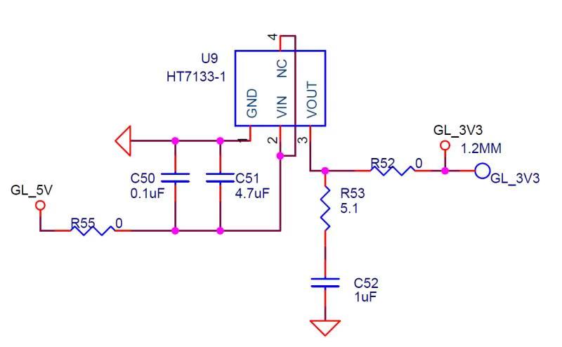
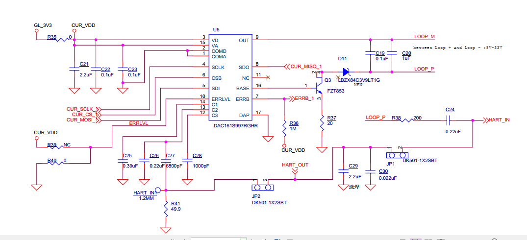
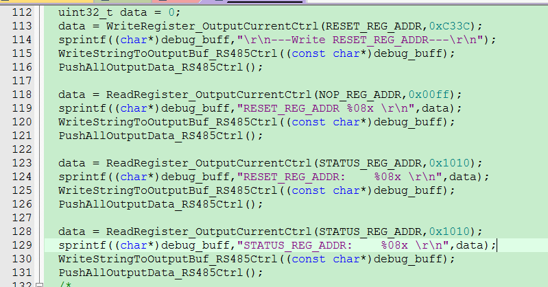
Below the first picture is the programming. One Write command, and three read command. And the CSB(blue), SDI(yellow), SDO(green), SCLK(pink) waveforms are as following. We can see that, the SDO still has no change. Could you please tel me the reason? The schematic is as below. In addition, about the timing requirement, in our datasheet the tZSDO(CSB falling edge to SDO valid) should be smaller than 35ns, but the cusomer's MCU can't meet this requirement. Is this fault related to the timing requirement?

Thanks & Best Regards,

Sherry

  • Hi Sherry,

    My colleague Kevin will get back to you tomorrow (the US is in holiday today).

    Thanks,

    Paul

  • Hi Kevin,

    I have some updates, the customer's system design and system schematic are as below, and the LDO2 in the system design is HT7133-1 in the schematic. When I test the loop current, the result is 0. Could you please answer three questions?

    1. Is the system design correct? They didn't use the loop power, but an external power.

    2. Why the loop current is 0?
    3. When the customer tries to read the status through SPI, they failed. When they write command through SPI, they failed, either. Could you please tell me the reason? about the timing requirement, in our datasheet the tZSDO(CSB falling edge to SDO valid) should be smaller than 35ns, but the cusomer's MCU can't meet this requirement. Is this fault related to the timing requirement?

    Thanks & Best Regards,

    Sherry

  • Hello All,

    I believe I saw this schematic before, though not all of it was shared. Specifically, how the GL_3V3 net was derived. Now, it is clear that this supply is coming from an isolated power supply.

    There is a bit of a conflict in the power domain of this design. The power return path is the "blank" ground symbol in this design, which is the same path that the loop-pass BJT is connected to. Separately there is the loop+ and loop- current loop. We do not know the relative potential difference from the loop receiver ground and the "blank" ground symbol in the schematic. Therefore, we cannot say with certainty where the current is flowing. For the design to function properly, power needs to be derived from the loop and the OUT pin connected to the return path.

  • Hi Kevin,

    I want to confirm two things,

    1. Our recommended solution is as below the first picture, the LDO's input comes from the loop power. And now the customer's solution is that LDO's input comes from the an isolated DCDC instead of loop power, and the schematic is as the second picture. And between the MCU and DAC161S997, the customer also adds optocoupler. The completed schematic I will send to your email.

    I think this solution is also ok, right?

    2. About the SPI timing, if I can't meet the requirements of below parameters, can the SPI work normally? tZSDO>35ns,tSDOZ<0. Please refer to the picture I sent in the first post. Now SDO's output is abnormal. I want to know whether this fault is related to these two parameters  tZSDO&tSDOZ.

    Thanks & Best Regards,

    Sherry

  • Sherry,

    Thank you for sending the confidential information via email while continuing the discussion here. This is helpful for the community at large, so I appreciate that.

    The issue is that by having the LDO powered by the isolated supply, the design has effectively created two current loops. The DAC161S997 expects all of the return current to be connected to the COMA and COMD pins and therefore go through the OUT pin. While COMA and COMD are connected to the GND symbol, the system-level view of things still creates two current loops since the GND pin (what I called "blank" GND previously) is referred to the isolated LDO source while the loop power / GND (what would be connected to LOOP+ and LOOP-). We don't know anything about the potential difference between LOOP- and GND or LOOP+ and the GL_3V3 net - which is probably what is creating the analog issues.

    Potentially this is impacting the digital as well. It is possible the device(s) have been damaged since we don't know anything about some of these potential differences the device is being exposed to.

  • Hi Kevin,

    Thanks for your reply!

    So I should suggest the customer to change the system design, right?

    In addition, could you please help answer the second question about the timing parameters in the last post?

    Thanks & Best Regards,

    Sherry

  • Sherry,

    I am not really sure what is going on with the oscilloscope captures you shared of their SPI bus. It looks like SDO is transitioning exactly with the SCLK which should not be the case as data should be stable and ready to be clocked out on the SCLK rising edges. Also even without a read command being issued the contents of SDO should be the previous frames SDI - which is not shown in those captures.

    My best guess is that potentially the device is not behaving correctly due to the issues we've previously discussed on the schematic level.

  • Hi Kevin,

    Thanks for your reply!

    I have applied for the EVM for this customer, and today we tested the EVM. Tomorrow the customer will try to use their SOC to control the  DAC161S997 of EVM. I will tell you once there is any update.

    Thanks & Best Regards,

    Sherry