This thread has been locked.

If you have a related question, please click the "Ask a related question" button in the top right corner. The newly created question will be automatically linked to this question.

TSW40RF82EVM: New configuration for TSW40RF82EVM

Part Number: TSW40RF82EVM

Hello,

Is it possible to make a new configuration for TSW40RF82 EVM board with only 1 input and 1 output.

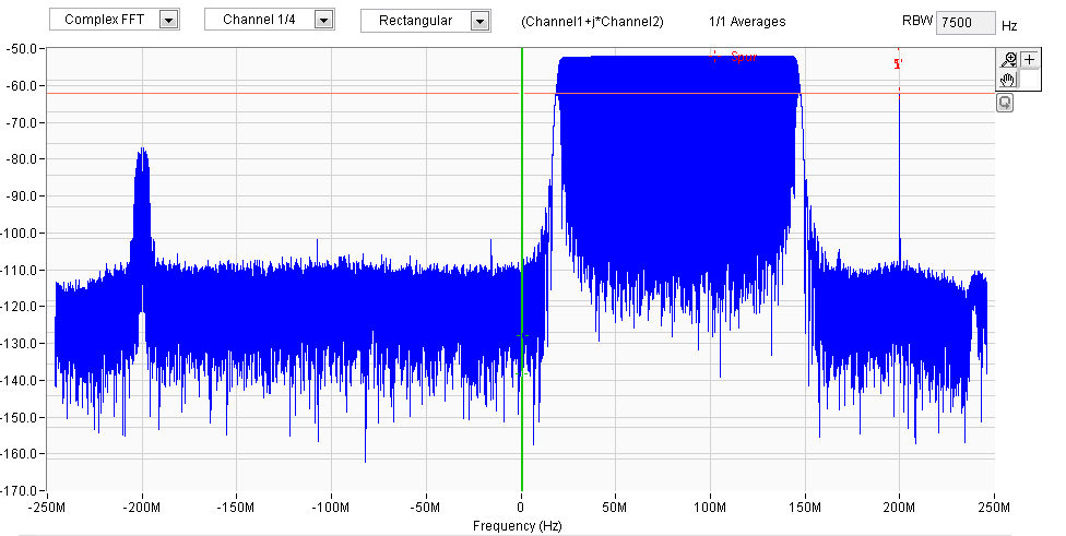
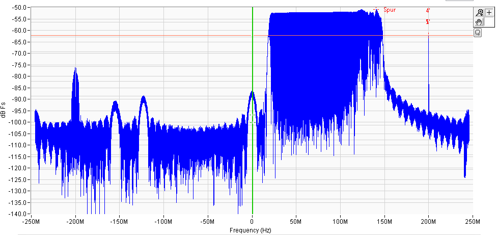
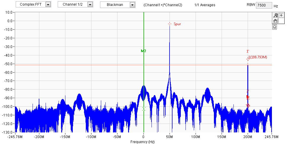
Currently I use 2T2R2T2R_RevC_ConstInput_6xDec_12xInt_2949p12M_5898p2_4915p2Gb and i would like same configuration but  more like 1T1R_RevC_ConstInput_6xDec_12xInt_2949p12M_5898p2_4915p2Gb.

Regards,

Damien

  • Damien,

    We are taking a look at this and will get back to you asap. 

    Yusuf

  • Hi Damien,

    Are you looking for a configuration where one 1 Transmit channel and 1 receive channel are powered down to reduce power consumption? 

    Regards,

    Vijay

  • Hi Vijay,

    Yes, i looking for a configuration where one 1 Transmit channel and 1 receive channel.

    Regards,

    Damien

  • Hi Damien,

    You can power off RX channel B of ADC32RF45 by adding the below lines at the end of config file:

    "

    ADC32RFxx_LOWLEVEL

    0x0012 0x04 // select MASTER page

    0x0039 0x52 // EN CHB PDN = 1

    0x0020 0x02 // CHB PDN = 1

    "

    I'll send the config to PDN TX channel B tomorrow.

    Regards,

    Vijay

  • Hi Damien,

    You can power off TX channel B of DAC38RF80 by adding the below lines at the end of config file:

    "

    DAC38RF8x

    0x40B 0x0006

    "

    By doing this, we can put DAC B to sleep. Here we set bit 2 of "register 0x0B in misc config registers page" to "1". Bit 1 of this register is already set to "1"

    Regards,

    Vijay

  • Hi Vijay,

    Sorry for the late reply.

    I try to make your modification but the capture don't work, i have this error message "TIMED_OUT_ERROR".

    I think, I use a wrong .ini file for this configuration. Can you tell me what .ini file I have to use for this configuration?

    Currently, I use this files :

    ADC32RF80_LMF_8411 and DAC38RF8x_LMF841

    Regards,

    Damien

  • Hi Damien,

    For DAC38RF8x, same ini file should work. For the ADC, ini file needs to be updated:

    The TSW capture card is currently programmed to look for valid JESD data on all 8 JESD lanes from ADC32RF45. When PDN chB is selected, only the top four lanes (lanes that carry chA output) will be active. So configuration file for TSW card has to be modified. Please follow the below steps to achieve this. 

    1. Program both ADC32RF45 and TSW capture card as described in the user's guide.
    2. If you are using TSW14J56 rev D capture card, copy the attached 'ADC32RF45_LMF_82820_only_chA.ini' to 'C:\Program Files (x86)\Texas Instruments\High Speed Data Converter Pro\14J56revD Details\ADC files' in your PC.
    3. In HSDC pro, click on Instrument options --> Disconnect from the Board. Connect to board again and select 'ADC32RF45_LMF_82820_only_chA' instead of 'ADC32RF45_LMF_82820'  
    4. Assert PDN chB En and PDN chB in ADC configuration tab in ADC32RFxx tab in GUI.
    5. In HSDC pro, click on Instrument options --> Reset board.
    6. Click on 'Capture' to capture data from chA 

    ADC32Rf80_LMF_8411_only_chA.txt
    [ADC]
    
    Interface name="TSW14J56REVD_AEQ_FIRMWARE"
    Number of channels=2
    Channel Pattern=1,2
    
    Data Postprocessing=1:32768
    \\operation:operand
    \\operaion
    \\0=bit shift
    \\1=xor
    \\2=and
    \\3=or
    \\4=not
    \\operand
    \\value(+ve if bitshift by right and -ve if bitshift by left)
    \\E.g 0:-2,1:1024
    \\bitshift by left 2 times and then xor by 1024
    Number of Bits=16
    Max sample Rate=3072000000
    Register_Config="-"
    \\[Register Address]:[Register Value]:[Number of Bytes to be sent as]
    DLL Version=1.0
    Read EVM Setup Procedure="EVM Setup Procedure not available"
    \\use <> as delimiter for newline
    
    [Version 1.0]
    
    Lane Rate Adjustment Factor= 1 // default = 1
    
    
    \\Lane Rate = N'(Fs)(10)(No Of Channels)(Lane Rate Adjustment Factor)/(L*8)
    
    JESD IP Core_CS=0
    JESD IP Core_F=1
    JESD IP Core_HD=0
    JESD IP Core_K=16
    JESD IP Core_L=4
    JESD IP Core_M=2
    JESD IP Core_N=16         
    JESD IP Core_NTotal=16   
    JESD IP Core_S=1
    JESD IP Core_SCR=0
    JESD IP Core_Tailbits=0
    JESD IP Core_LaneSync=1
    JESD IP Core_Subclass=1
    
    
    MIF Config= 0.611G to 1.5G:RX:RX_PMA_x10,1.5G to 12.5G:RX:RX_PMA_x40
    
    \\List of Lane Rate Range,PLL Type and their MIF File names that needs to be configured,separated by ":"
    \\These MIF Files need to be present under MIF Files Folder
    
    Fabric PLL Counter = 0.611G to 1.5G:0x080808,1.5G to 12.5G:0x080202  \\ was 080202
    
    Invert Sync Polarity = 1 
    \\Invert Sync polarity, 1:invert; 0: do not invert
    Invert Serdes Data = 0  
    \\Invert Serdes Data, 1:invert; 0: do not invert
    Transceiver Mode = 0  
    \\1:xcvr mode; 0: TX/RX only mode
    
    
    Lane Mapping=lane0:7,lane1:4,lane2:6,lane3:5,lane4:3,lane5:0,lane6:2,lane7:1
    
    
    \\lane = device pin, :# JESD spec lane
    \\ example  lane0:7  = DA0 of device is mapped to lane 7 of JESD SPEC
    
    \\Lane pattern for the LMF modes
    Group 128 bits Flag = 1
    \\If 1, will group 128 bits from each DDR, and then apply the channel pattern
    \\If this parameter is not present, it will follow the earlier mode used in v2.40
    Bit Packing = 1
    \\0 - Data are not bit packed. 
    \\1 -  Data are bit packed(MSB aligned) without any padded zeroes
    
    \\ sample from lane 0, sample from lane 1, sample from lane 0, sample from lane 1...4 times then sample from lane 2, sample from lane 3.....


    Bit Packing Channel Pattern = C1S1[15:8],C1S2[15:8],C1S3[15:8],C1S4[15:8],C1S1[7:0],C1S2[7:0],C1S3[7:0],C1S4[7:0],C2S1[15:8],C2S2[15:8],C2S3[15:8],C2S4[15:8],C2S1[7:0],C2S2[7:0],C2S3[7:0],C2S4[7:0]

    Regards,

    Vijay

  • Hi Vijay,

    Now the system work with 1 channel thank you for that, but i observe some differences on spectral resultat.

    Before the new configuration I have this resultat:

    With the new configuration I have this :

    Maybe others parameters must be modify, for have a same result?

    Do you have an idea?
    Regards,
    Damien
  • Hi Damien,

    Your DAC output is as expected and you have problem with ADC only. Please confirm?

    For the ADC powering down chB is not expected to affect chA output.

    Can you run default (2T2R) config and make sure FFT is looks okay and then run config to PDN chB:

    "

    ADC32RFxx_LOWLEVEL

    0x0012 0x04 // select MASTER page

    0x0039 0x52 // EN CHB PDN = 1

    0x0020 0x02 // CHB PDN = 1

    "

    To make sure this issue is caused by powering down channel B.

    Also if you confirm the above, please send an FFT plot with single tone input. This will help me better understand the issue.

    Regards,

    Vijay

  • Hi Vijay,

    I confirm the DAC ouput is as expected and the FFT is okay with default (2T2R) config.

    But I try to make  your test what you ask but I don't make it work. I have a error message.

    I make a new config file where i add your modification, after that I make exactly the same thing with the default 2T2R config and I have a error message, when I click on capture.

    What I make wrong?

    Regards,

    Damien

  • Hi Damien,

    After you make the modification, when you try to capture are you selecting the below ini file?

    'ADC32RF45_LMF_82820_only_chA'

    Regards,

    Vijay

  • Hi Vijay,

    You have right i don't use 'ADC32RF45_LMF_82820_only_chA' for my test, sorry for that.

    With this configuration I have this FFT :

    And with the default configuration I have this expected FFT:

    Regards,

    Damien

  • Hi Damien,

    As you were using ADC32RF80_LMF_8411, you can use the attached ADC32RF80_LMF_8411_only_chA.

    1. Copy the attached ini file to C:\Program Files (x86)\Texas Instruments\High Speed Data Converter Pro\14J56revD Details\ADC files. Close an reopen HSDC Pro.

    2. In select ADC drop-down menu, select ADC32RF80_LMF_8411_only_chA instead of ADC32RF80_LMF_8411.

    The earlier ini file I sent you was for a different JESD mode. That's the reason for bad FFT.


    Regards,

    Vijay


    ADC32RF80_LMF_8411_only_ChA.ini

  • Hi Vijay,

    The problem is not resolve, now i have this FFT :

    In the new ini file you send me, i make a modification I active the tranceiver mode = 1 

    Regards,

    Damien

  • Damien,

    Can you send me the original ini that you were using for capturing both the ADC channels (one with which you get the right output)?

    Can you double check that you are selecting ADC32RF80_LMF_8411_only_ChA in the 'select ADC' drop-down?

    I have verified that the ini file I sent on my setup again and it works as expected. 

    Regards,

    Vijay

  • Hi Vijay,

    I attached the ini file with which i get the right output.

    I double checked and ADC32RF80_LMF_8411_only_ChA file is well selected.

    ADC32RF80_LMF_8411.txt
    [ADC]
    
    Interface name="TSW14J56REVD_AEQ_FIRMWARE"
    Number of channels=4
    Channel Pattern=1,2,3,4
    
    Data Postprocessing=1:32768
    \\operation:operand
    \\operaion
    \\0=bit shift
    \\1=xor
    \\2=and
    \\3=or
    \\4=not
    \\operand
    \\value(+ve if bitshift by right and -ve if bitshift by left)
    \\E.g 0:-2,1:1024
    \\bitshift by left 2 times and then xor by 1024
    Number of Bits=16
    Max sample Rate=3072000000
    Register_Config="-"
    \\[Register Address]:[Register Value]:[Number of Bytes to be sent as]
    DLL Version=1.0
    Read EVM Setup Procedure="EVM Setup Procedure not available"
    \\use <> as delimiter for newline
    
    [Version 1.0]
    
    Lane Rate Adjustment Factor= 1 // default = 1
    
    
    \\Lane Rate = N'(Fs)(10)(No Of Channels)(Lane Rate Adjustment Factor)/(L*8)
    
    JESD IP Core_CS=0
    JESD IP Core_F=1
    JESD IP Core_HD=0
    JESD IP Core_K=16
    JESD IP Core_L=8
    JESD IP Core_M=4
    JESD IP Core_N=16         
    JESD IP Core_NTotal=16   
    JESD IP Core_S=1
    JESD IP Core_SCR=0
    JESD IP Core_Tailbits=0
    JESD IP Core_LaneSync=1
    JESD IP Core_Subclass=1
    
    
    MIF Config= 0.611G to 1.5G:RX:RX_PMA_x10,1.5G to 12.5G:RX:RX_PMA_x40
    
    \\List of Lane Rate Range,PLL Type and their MIF File names that needs to be configured,separated by ":"
    \\These MIF Files need to be present under MIF Files Folder
    
    Fabric PLL Counter = 0.611G to 1.5G:0x080808,1.5G to 12.5G:0x080202  \\ was 080202
    
    Invert Sync Polarity = 1 
    \\Invert Sync polarity, 1:invert; 0: do not invert
    Invert Serdes Data = 0  
    \\Invert Serdes Data, 1:invert; 0: do not invert
    Transceiver Mode = 1  
    \\1:xcvr mode; 0: TX/RX only mode
    
    
    Lane Mapping=lane0:7,lane1:4,lane2:6,lane3:5,lane4:3,lane5:0,lane6:2,lane7:1
    
    
    \\lane = device pin, :# JESD spec lane
    \\ example  lane0:7  = DA0 of device is mapped to lane 7 of JESD SPEC
    
    \\Lane pattern for the LMF modes
    Group 128 bits Flag = 1
    \\If 1, will group 128 bits from each DDR, and then apply the channel pattern
    \\If this parameter is not present, it will follow the earlier mode used in v2.40
    Bit Packing = 1
    \\0 - Data are not bit packed. 
    \\1 -  Data are bit packed(MSB aligned) without any padded zeroes
    
    \\ sample from lane 0, sample from lane 1, sample from lane 0, sample from lane 1...4 times then sample from lane 2, sample from lane 3.....


    Bit Packing Channel Pattern = C1S1[15:8],C1S2[15:8],C1S3[15:8],C1S4[15:8],C1S1[7:0],C1S2[7:0],C1S3[7:0],C1S4[7:0],C2S1[15:8],C2S2[15:8],C2S3[15:8],C2S4[15:8],C2S1[7:0],C2S2[7:0],C2S3[7:0],C2S4[7:0],C3S1[15:8],C3S2[15:8],C3S3[15:8],C3S4[15:8],C3S1[7:0],C3S2[7:0],C3S3[7:0],C3S4[7:0],C4S1[15:8],C4S2[15:8],C4S3[15:8],C4S4[15:8],C4S1[7:0],C4S2[7:0],C4S3[7:0],C4S4[7:0]

    Regards,

    Damien

  • Hi Damien,

    The only difference in the above ini files is changing from 2 channels to 1 channel. I don't understand why FFT is different. To debug this, can you please do the below test.?

    1. Bringup the EVM as per user guide (both channel ON; using ADC32RF80_LMF_8411 ini file)

    2. You should get expected FFT output.

    3. In HSDC Pro select one channel ini file (ADC32RF80_LMF_8411_only_chA)

    4. Press capture (you can capture only chA with this ini) and check if the FFT output as expected.

    Note that we are not doing the chB power down SPI writes to ADC32RFxx in the above process. This test is to help understand if the issue is in data processing in HSDC pro. 

    Regards,

    Vijay

  • Hi Vijay,

    I make the test you ask me and when I use ADC32RF80_LMF_8411 ini file the FFT is as expected. But when I use ADC32RF80_LMF_8411 ini file the FFT is like this :

    Regards,

    Damien

  • Hi Damien,

    I verified both the ini files you sent and the differences are only for changing from two channels to single channel.

    I also verified on my setup that both ini files function as expected.

    I get the same output (in picture above) from channel A weather I use "ADC32RF80_LMF_8411.ini" or "ADC32RF80_LMF_8411_only_ChA.ini"

    It is not expected to get any difference between the two files.

    Regards,

    Vijay

  • Hi Vijay,

    Ok, maybe I use a wrong setting in the software HSDC pro and TSW40RF8x EVM GUI.

    In HSDC pro I make this :

    In ADC tab : I load ADC32RF80_LMF_8411.ini or ADC32RF80_LMF_8411_only_chA.ini,

    In setting ADC Output Data rate : ADC Sampling Rate 2.94912G, NCO = 199.98M, Decimation 6

    In DAC tab : Data Rate (SPS) = 491.52M

    In DAC tab : I load this pattern : 4ch_64freq.csv

    In TSW40RF8x EVM GUI I make this:

    - In Low Level View tab : I load 2T2R_RevC_ConstInput_6xDec_12xInt_2949p12M_5898p2_4915p2Gb.cfg file

    - In DAC38RF8x tab, Quick start tab : M = 4, Desired interpolation = 12x and I click on "PLL AUTO TUNE" button

    - In DAC38RF8x tab, DAC38RF8x under tab, Digital(DAC A) and Digital(DAC B) : NCO Frequency(Mhz) = 199.98, uncheck Constant input and i click on "Update NCO" button

    - In ADC32RFxx tab, ADC32RFxx under tab, DDC configuration under tab : ChA DDC0 NCO1 = 4444, ChB DDC0 NCO1 = 4444

    - In DAC38RF8x tab, Quick start tab :I click on " Reset DAC JES cor & SYSREF TRIGGER" button

    Can you use my pattern and confirm if the FFT is as expected?

    Can you say me if I make some mistake in configuration of Software?

    Regards,

    Damien 

  • Hi Damien,

    I was testing the ADC ini files on an ADC32RF45EVM. As both of us are using TSW14J56 capture card, the results are expected to be same. But as you are using TSW40RF82EVM, I'll setup the same EVM and try your test. I'll get back to you with results ASAP.

    Meanwhile can you test with single tone instead of pattern file and see if there's a difference in results between two ini files?

    Are you connecting the TX output as RX input in the FFT plots you sent me?

    Regards,

    Vijay

  • hi Vijay,

    Yes, I connect the TX output as RX input.

    I realize your test and the result is not the same when I change the ini files.

    The single tone I make is : Tone BW = 1, # = 1, Tone Center 50M, Tone selection = Complex

    I have this FFT with ADC32RF80_LMF_8411.ini file:

    I have this FFT with  ADC32RF80_LMF_8411_only_chA.ini file:

    Regards,

    Damien

  • Hi Damien,

    I was able to replicate this issue on my setup.

    When you use the ADC32RF80_LMF_8411_only_chA.ini, the capture depth should be limited to 32768 samples. To change this,

    In HSDC pro ADC tab in top menu bar, click on 'Data Capture Options' -> 'Capture Option', change the '# samples' from 65536 to 32768.

    Click OK. 

    After this change when you capture, the FFT should be as expected.

    Regards,

    Vijay

  • Hi Vijay,

    Yes, if I limite the number of samples as 32768 the FFT is as expected.

    Can you explain me this limitation? 

    Is it possible to rise this limitation?

    Regards,

    Damien

  • Hi Damien,

    There are limitations from FPGA timing constraints in transceiver mode. I will check with our FPGA firmware team to understand the limitation. I'll get back to you ASAP.

    Note that it is proven that the issue is on FPGA side and not from ADC or DAC, 

    Regards,

    Vijay

  • Hi Damien,

    The constraint arises when simultaneously reading from and writing into DDR memory by the FPGA. In case where we changed ini file of ADC to one channel but using two channel ini for DAC, the read rate from DDC is different from write rate which causes the issue.

    So I tried changing the DAC side ini to one channel too. With that I'm able to capture higher number of samples without the FFT issue.

    Copy the attached ini file to C:\Program Files (x86)\Texas Instruments\High Speed Data Converter Pro\14J56revD Details\DAC files in your PC. By using this ini for DAC, you can run in 1T1R mode and capture more number of samples. 

    DAC38RF8x_LMF_841_only_chA.ini

    Regards,

    Vijay

  • Hi Vijay,

    Thank you for your help now is work fine.

    Regards,

    Damien