This thread has been locked.

If you have a related question, please click the "Ask a related question" button in the top right corner. The newly created question will be automatically linked to this question.

ADS1282: Noise in ADC Data

Part Number: ADS1282

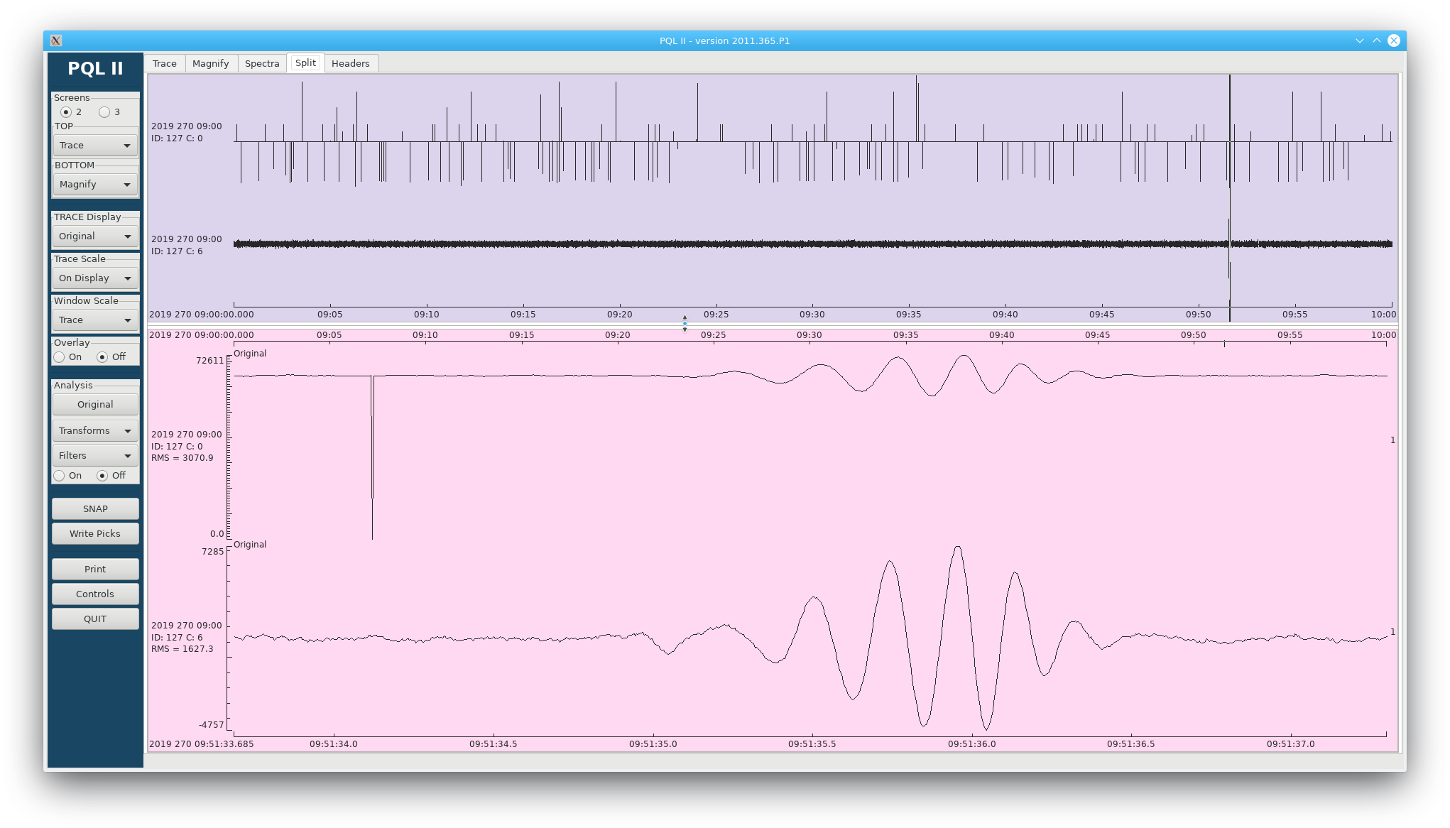
I am designing a data logger for geophysical applications using the ADS1282. I already build several prototype boards for lab and field testing. The initial field test showed a considerable amount of noise as shown in the attached figures. The top half of the figure (with title PQLII) shows an overview of data recorded by the prototype logger (top trace) and an old logger using a Cirrus Logic ADC (bottom trace) . The sensor connected to both data loggers is a vertical geophone. The bottom half shows an event detected by the sensors.  The recorded signal by the ADS1282 logger is as expected and comparable to the signal recorded by the old logger. However, this figure also shows that the prototype logger is noisy. Several voltage spikes can be observed in the overview trace at the top of the figure. As can be seen from the second trace, the old logger is free of this noise. The data was collected on the field and both loggers were deployed in the same area, thus eliminating the environment as the source of the noise. The both the prototype and old loggers use the same MCU and the same power regulators. Have you seen noise like this in any other design using the ADS1282? Could noise like this be caused by errors in reading data from the ADCs?

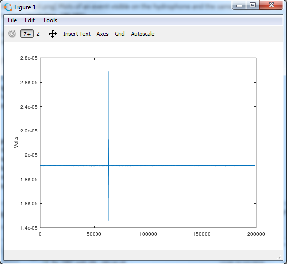
The other figure (Figure 1) shows data recorded when the input to the ADS1282 is connected to the internal 400 Ohm resistors. In this a single instance of a large voltage spike is observed. In general, data recorded in lab tests still show this noise albeit with a lower number of occurrences than in the field test. Any suggestions about what may be the source of this noise. So far I have tried, shielding the ADC board from the MCU and Power boards and the noise is still present. 

Thank you.

Best regards, 

Alex

  • Hi Alejandro,

    Welcome to the E2E forum!  Noise is a common issue with ADCs and can be difficult to troubleshoot.  This can be especially true with prototyping situations.  Often the noise is picked up in cabling from board interconnections (wiring) and from improper termination of analog inputs.  EMI and RFI are possible contributors as well as power line-cycle pickup.  If you can send me your schematic and board layout I can help by reviewing them.

    Best regards,

    Bob B

  • Dear Bob,

    Thank you for your prompt reply. Is there a way to send the schematic and board layout in a confidential manner? Thank you.

    Best regards,

    Alex

  • Hi Alex,

    You can contact me in a couple of ways and both are private.  One is to click on my icon in E2E and then start a conversation and attach a zip file of the files you wish to send me.  The second method is to send the zip file to the email address:

    pa_deltasigma_apps@ti.com

    Best regards,

    Bob B

  • Chris Hall,

    Your colleague Bob Benjamin mentioned that he forwarded you the files relating to this issue. Have you been able to review them? Thank you

    Best regards,

    Alex

  • Hi Alex,

    Thanks for your patience!

    Yes, I've looked over the schematic and layout...

    Nothing stood out to me as as an issue from schematic. I noticed that you have multiple ADC channels though. Do you know if the observed noise spike is present on multiple channels or is it generally a problem with only a single ADC channel?

    On the layout, I did notice some potential issues with the clock trace routing... The clock traces (CLK and SCLK) are routed through multiple vias and cross (over or under) clock traces on other PCB layers. I can't know for sure if this is an issue or not, but it could be causing some signal integrity issues and bad ADC readings. I would recommend probing some of the SPI signals on the input end (i.e. the receiving side that is not driven) to see if there are any hints of clock coupling, ringing, or other signal integrity issues.


    If it would be possible to get more information about the ADS1282 register settings, the sequence of SPI commands sent to the device, and perhaps a data file showing some of the noise spikes that could also be helpful for troubleshooting this issue.

  • Hi Chris,

    Regarding the noise spike, the system is still in prototype stage and the multi-channel version of the CPLD software is not completed ready. Therefore, all the measurements up to now have been single channel. However, the noise spike appears in every channel. I have run tests on every channel and the noise has appeared in all of them.  

    After power up, the following commands are sent to configure the ADC:

    0x11         - SDATAC to stop conversions

    0x410042 - WREG (1 byte) Sample rate: 250 samples per second

    0x42000E - WREG (1 byte) PGA gain: 64

    0x410046 - WREG (1 byte) Set digital filter to: Minimum Phase

    0x42002E - WREG (1 byte) Set Mux select to: Internal short via 400 Ohms

    0x11          - SDATAC

    0x04          - SYNC

    0x10          - RDATAC

    wait for nDRDY to go LOW

    0x11          - SDATAC

    0x60          - OFSCAL command

    0x10          - RDATAC 

    record a few minutes of data to verify Offset Calibration

    0x11          - SDATAC

    0x42000E - WREG (1 byte) Set Mux select to: AINP1 and AINN1

    0x10          - RDATAC to start conversions

    I attach a couple of data files. The file named "adc1_voltage_cal_16.log" corresponds to data recorded immediately after calibration (i.e. with the Mux select still set to internal short via resitors). The file named "adc1_voltage_cal_19.log" corresponds to data recorded with the Mux select set to AINP1 and AINN1. The input signal is 10 mV from a bench power supply, which is, presumably, the source of the 50Hz noise. 

    I will probe the SPI signals as you recommend to check for any signal integrity issues. Thank you.

    Best regards,

    Alex

    adc1_voltage_cal_16.logadc1_voltage_cal_19.log 

  • Dear Chris,

    I must add that both previous data files show an instance of the noise spike. 

    Regards,

    Alex

  • Hi Alex,

    Wow... you got a very consist bit flip of bit #27 occurring every 250 samples (i.e. once a second). Is there anything in your system with a 1 Hz period, such as a GPS clock for example, that you can try disabling to see if the noise spike goes away?

    With such a consistent error, hopefully there is a way you can trigger your oscilloscope to capture the SPI data during this event to see if the issue is with the ADC (outputting bad data) OR with noise coupling into the SPI signals and causing the MCU to read an invalid result. You might need to try probing the DOUT and SCLK signals at both ends (the digital output and digital input sides on the corresponding ADC and MCU pins) to see if there is any difference. Sometimes the high-impedance end of the trace can show a different voltage waveform on an oscilloscope.

  • Hi Chris,

    Apologies. I should have explained the data format of the files I sent. The file already has the data format that we use for the multi-channel system. The first byte is a status byte and the following 3 bytes are data. We are using 24-bit resolution. We drop the 8 (including redundant sign bit) least significant bits from the ADC's 32-bit data output. The status byte contains the status for MFLAG, the channel ID, an event flag, and an overflow flag. 

    BIT 7: MFLAG 

    BIT 6: UNUSED (set to 0)

    BIT 5: CH[1]

    BIT 4: CH[0]

    BIT 3 : UNUSED (set to 0)

    BIT 2: event flag

    BIT 1: UNUSED (set to 0)

    BIT 0: OVRFLW

    At the moment the event flag bit is set every time the system receives the pulse per second signal that is used to timestamp the samples.

    I will do a single channel test eliminating all unessential clock signals. I will let you know the results of this test. Thank you.

    Best regards,

    Alex