This thread has been locked.

If you have a related question, please click the "Ask a related question" button in the top right corner. The newly created question will be automatically linked to this question.

ADS1115: Aquisition time, conversion time and discharge time

Part Number: ADS1115

Hello Team

I am working on a system for pairing and selection of optocouplers. I work with 8 optocouplers per test cycle and I use 2 ADS1115's single ended in continuos mode at 860sps. After a settling period of 15 secs all 8 channels are measured, waiting 3ms after each input switch. This pattern is repeated 10 times and the results are averaged. 860sps is chosen because all 80 measurements must be done within less than ½ sec. This setup does function ok, but some noise is introduced from the opamps in the signal conditioning circuitry, so I intend to add a unity gain buffer with RC lowpass filter to each channel.

As a SPICE model of the ADS1115 cannot be found I would like to make a simulation model of the ADC input to help me choose the best opamp/filter combination, and for this job I need some information.

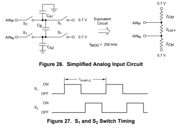
 As I understand from the datasheet the sampling frequency is 250KHz giving a total sample time of 4 microseconds. In this period we will have an aquisition period, a hold or conversion period and finally a discharge period. I suppose this pattern is repeated many times during the 1.1ms needed for the 860sps and then averaged ?

What I would like to know is:

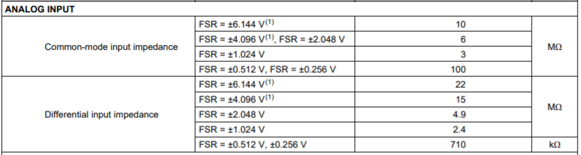
1. the aquisition time     2. the conversion time     3. the discharge time    4. the timing between the three.  and  5. the values of the capacitors in the input.

Thank you very much in advance

Ole Palmhoej 

  • Ole,

    The ADS1115 is basically a delta-sigma type of ADC. In this type of device, the input voltage is sampled repeatedly with an input sampling capacitor at a set modulator rate. After that it takes a set number of modulator cycles to get an ADC data. From the external point of view, the input samples the voltage at 250kHz and discharges it into a set voltage. You can see the basic structure on page 16 of the datasheet. The tSAMPLE is 1/fMOD.

    Each modulator cycle contains a charge and discharge. The conversion is done over the entire length of the data period. For the ADS1115, the input sampling capacitor value is dependent on the FSR setting of the device. This has the effect of giving an equivalent input impedance to depending on the FSR setting. This is listed in the Electrical Characteristics Table on Page 7.

    You'll need to confirm the values, but I believe that the sampling capacitors vary from about 6pF at the smallest FSR to about 0.5pF at the largest FSR with some variance for parasitic capacitances and charge and discharge methodology.

    Joseph Wu

  • Thank you, Joseph, for your answer. Nice to get those capacitors right.

    The timing, however, remains to be solved. The most important time is the time where S1 is ON. That is the time where the sampling capacitor is charged, ie what I call the acquisition time. Within this period the input voltage will need to be completely settled, preferably within ½LSB error.

    While the oversampling of the delta sigma converter is good for reducing the impact of noise, the very short acquisition time is a challenge, and more so with an added RC filter in the input. The driver will have to overcome the kick back voltage drop as well as the minimum 5tau of the filter while fighting every tendency of ringing within perhaps 1.5 microseconds.

    That's why a useable simulation of the input really depends on the correct timing, and sadly this timing can not be found in the datasheet.

    I really hope you can help..

    Best regards

    Ole

  • Ole,


    I don't have specific design information on this. However, based on the way we've done some of our previous clocks, and non-overlapping clock structures for sampling and discharge, I could make a guess. The switch timing shown in Figure 27 shows a tSAMPLE of 250kHz. That would be 4us for the period. My guess is that the ON period for S1 and S2 would be about half that value minus 50ns for non-overlapping as a maximum (it should probably be around 20ns). That would be about 1.95us.


    Joseph Wu

  • Thank you very much

    Ole