This thread has been locked.

If you have a related question, please click the "Ask a related question" button in the top right corner. The newly created question will be automatically linked to this question.

ADS1293EVM: Gain/amplification factor not equal to 3.5x and varies with frequency

Part Number: ADS1293EVM
Other Parts Discussed in Thread: ADS1293, ALLIGATOR

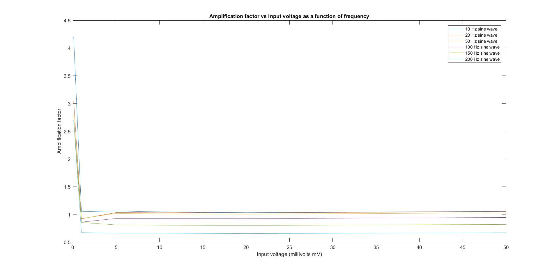
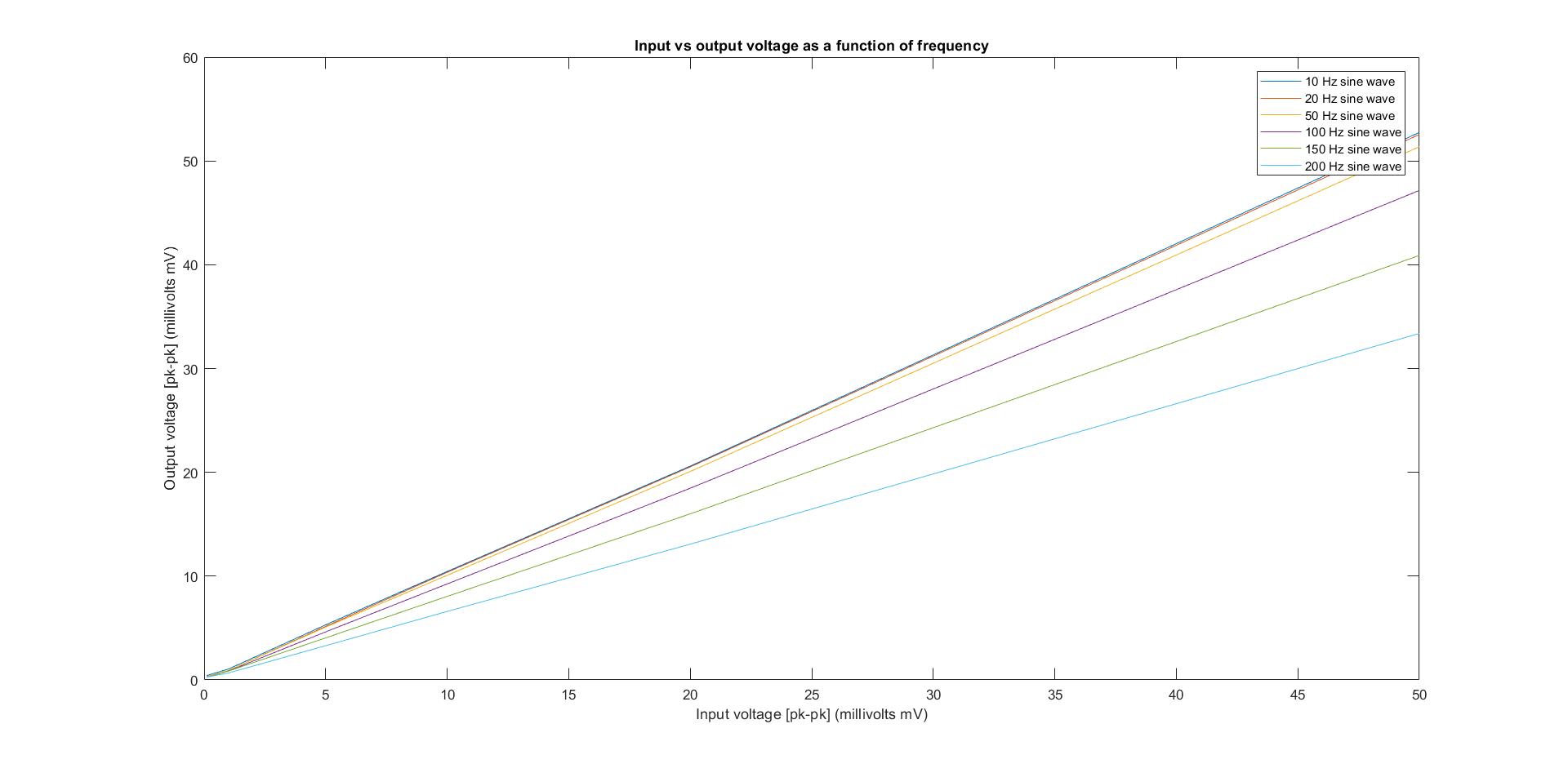
Hello. I have been using the TI ADS1293EVM board to acquire signals from a USB waveform generator (Analog Discovery module from Digilent [https://reference.digilentinc.com/reference/instrumentation/analog-discovery/start?redirect=1]). I performed a voltage (from 0.1 mV - 50 mV pk-pk sine wave with 0V offset) and frequency sweep (from 10 - 200 Hz) to characterise the ADS1293EVM.

I find that the amplification factor/gain of the ADS1293EVM varies as a function of frequency and is not equal to the value of 3.5x as mentioned on page 15 of the ADS1293 datasheet. Is this normal/expected or am I doing something wrong? I measured the output from the waveform generator using a scope and the voltages were what I expected them to be.

I have attached a couple of figures as well as a CSV file of the data I measured. The values of mean and pk-pk output voltage measured are obtained from the ADS1293 software's "Measurement" tab.

Thanks and regards,

Ganesh Raam

  Data-logging-19-04-20.csv

  • Hi Ganesh,

    There are a few things that could be happening here, but it sounds like a signal generator issue. Typically, as the frequency approaches the max for the signal generator, it becomes harder and harder for the signal generator to drive that voltage. So if the signal generator is rated for 217Hz, in order to actually get 50mV @ 200Hz, you may need to program 75mV @ 200Hz in order to actually see 50mV @ 200Hz on the output.

    Furthermore, you will need some resistance on the output of the signal generator for the ADS1293 to measure across. What is the value of this resistance?  

    Are you measuring the output from the discovery module while the ADS1293 is connected and active?

    What is the sample rate of the ADS1293? 

    I see in the excel sheet that the bandwidth is 217Hz, where is this coming from? 

  • Hello Alexander,

    Thanks for replying. I have answered your queries below.

    1) The Discovery module's signal generator can go up to 5V amplitude & 10 MHz frequency so I'm not sure if that could be a reason.

    2) Since I currently do not have access to resistors (due to Covid-19 and inaccessibility to labs), I am directly connecting the signal generator output to the ADS1293 input terminals (via a DB9 connector). Due to the high input impedance of the ADS1293 amplifier inputs, I assumed that the voltage across the ADS1293 should at least be higher than the output voltage at the signal generator (assuming that the series resistance of the signal generator is 50 ohms) but this does not seem to be the case. Is my assumption incorrect?

    3) Yes, I am measuring output from Discovery module when the ADS1293 is connected and active. When the input from the Discovery module is turned off, I get voltages in the range of a few hundred uV/ few mV when measured across the ADS1293.

    4) I am sampling the ADS1293 Channel 1 at 1066 SPS and I got the corresponding bandwidth as 213 Hz (not 217 Hz, typo in the Excel sheet) from the ADS1293 software's Data performance tab (I've attached a screenshot).

    I have also included the configuration ".xml" file and the corresponding register map ".csv" file used for data acquisition.

    Best regards,

    Ganesh

     data-acq-19Apr2020.csv

    data-acq-19Apr2020.xml
    <?xml version="1.0" encoding="UTF-8"?>
    <SensorAFE_config version="1.2.3(build 2)" device_name="LMP90507">
        <sensors_list/>
        <registers_list>
            <register address="0x00" value="0x00"/>
            <register address="0x01" value="0x11"/>
            <register address="0x02" value="0x00"/>
            <register address="0x03" value="0x00"/>
            <register address="0x04" value="0x00"/>
            <register address="0x05" value="0x00"/>
            <register address="0x06" value="0x00"/>
            <register address="0x07" value="0x07"/>
            <register address="0x08" value="0xff"/>
            <register address="0x09" value="0x00"/>
            <register address="0x0a" value="0x00"/>
            <register address="0x0b" value="0x00"/>
            <register address="0x0c" value="0x00"/>
            <register address="0x0d" value="0x00"/>
            <register address="0x0e" value="0x00"/>
            <register address="0x0f" value="0x00"/>
            <register address="0x10" value="0x00"/>
            <register address="0x11" value="0x00"/>
            <register address="0x12" value="0x04"/>
            <register address="0x13" value="0x00"/>
            <register address="0x14" value="0x00"/>
            <register address="0x15" value="0x00"/>
            <register address="0x16" value="0x00"/>
            <register address="0x17" value="0x05"/>
            <register address="0x18" value="0x00"/>
            <register address="0x19" value="0x00"/>
            <register address="0x1a" value="0x00"/>
            <register address="0x1b" value="0x00"/>
            <register address="0x1c" value="0x00"/>
            <register address="0x1d" value="0x00"/>
            <register address="0x21" value="0x01"/>
            <register address="0x22" value="0x02"/>
            <register address="0x23" value="0x02"/>
            <register address="0x24" value="0x02"/>
            <register address="0x25" value="0x00"/>
            <register address="0x26" value="0x00"/>
            <register address="0x27" value="0x08"/>
            <register address="0x28" value="0x00"/>
            <register address="0x29" value="0x00"/>
            <register address="0x2a" value="0x00"/>
            <register address="0x2b" value="0x00"/>
            <register address="0x2c" value="0x00"/>
            <register address="0x2d" value="0x00"/>
            <register address="0x2e" value="0x33"/>
            <register address="0x2f" value="0x10"/>
            <register address="0x30" value="0x00"/>
            <register address="0x31" value="0x00"/>
            <register address="0x32" value="0x00"/>
            <register address="0x33" value="0x00"/>
            <register address="0x34" value="0x00"/>
            <register address="0x35" value="0x00"/>
            <register address="0x36" value="0x00"/>
            <register address="0x37" value="0x00"/>
            <register address="0x38" value="0x00"/>
            <register address="0x39" value="0x00"/>
            <register address="0x3a" value="0x00"/>
            <register address="0x3b" value="0x00"/>
            <register address="0x3c" value="0x00"/>
            <register address="0x3d" value="0x00"/>
            <register address="0x3e" value="0x00"/>
            <register address="0x3f" value="0x00"/>
            <register address="0x40" value="0xff"/>
            <register address="0x50" value="0x00"/>
            <register address="0x60" value="0x00"/>
            <register address="0x62" value="0x00"/>
        </registers_list>
    </SensorAFE_config>
    

  • Hi Ganesh,

    1) I agree

    2) I would actually expect a drop here. However, I do believe putting a resistor across the terminals may help. 

    3) With the output from the discovery module turned off, the ADS1293 is converting noise on the inputs to the outputs. This makes sense. 

    4) The bandwidth of 213Hz is very close to your max frequency of 200Hz. Bandwidth is typically specified for -3dB at the rated frequency, attenuation will start to be seen much earlier. Trying increasing the bandwidth of the measurement and see if that helps.  

  • Hello Alexander,

    Thanks for your reply. Apologies for my late response.

    I was mistaken in thinking that the voltage would increase. As mentioned on page 5 of the ADS1293 datasheet, the differential input resistance is around 500 Mohm and hence a drop in the voltage will be expected as you had mentioned.

    I connected a load resistance and connected the ADS1293EVM's inputs across the load resistance. This time, in order to bypass the DB9 connector, I directly connected the wires from the load resistance to the test points (IN1 and IN2) via alligator clips. I repeated the experiment with multiple load resistances (50 ohm, 100 ohm, 1k, 10k ohm) as well. I still face the same problem that the gain is not 3.5x and that the amplitude of the measured voltage (45 mV pk-pk) is lower than that of the input voltage (50 mV pk-pk) for a sine wave input (between 20 and 150 Hz). Is there a specific range of load resistance values that you would recommend?

    Best regards,

    Ganesh Raam

  • Hi Ganesh,

    As I mentioned in my previous posts, please try increasing the bandwidth as the signal is most likely being attenuated. 

  • Hello Alexander,

    In my first post, I had attached images where the frequency of the input voltage was as low as 10 Hz but the problem still existed. I did also repeat the test with different values of bandwidth (as high as ~600 Hz) but changing the bandwidth did not seem to make a difference.

    However, I did find this post on the TI community (http://e2e.ti.com/support/data-converters/f/73/t/432687?ads1293-output) regarding the correct biasing of the ADS1293 INA. I have the following questions based on the post.

    1. What would be the correct way to bias the INA of the ADS1293EVM when connecting signal generator voltages as INA inputs? I am currently leaving the RLD amplifier output floating/disconnected. Is it okay to leave the RLD amplifier powered down and disconnected? In this post (https://e2e.ti.com/support/data-converters/f/73/p/484297/1748167),  mentions that leaving the RLD disconnected would imply that the INA inputs are left floating. But in this post (https://e2e.ti.com/support/data-converters/f/73/p/734675/2721447),  mentions that it is okay to leave the RLDOUT pin floating and the RLD amplifier powered down on the ADS1293.

    2. Should the output of the RLD amplifier be connected to the GND of the signal generator by routing the SELRLD to the corresponding input terminal using the flexible routing switch on the ADS1293 software. Or should the RLDOUT test pin on the ADS1293EVM board be connected to the GND of the signal generator?

    Thanks and regards,

    Ganesh Raam

  • Hi Ganesh,

    Mid-supply is typically the DC point for biasing the input of a PGA/INA.

    Using RLD to connect to the GND of the signal generator would be fine, alternatively you could simply add a DC offset.