This thread has been locked.

If you have a related question, please click the "Ask a related question" button in the top right corner. The newly created question will be automatically linked to this question.

ADS124S08: Thermal Pad Plating Thickness?

Part Number: ADS124S08
Other Parts Discussed in Thread: ADS1235-Q1, LM53600-Q1

This is a not often seen request, but I have a customer asking me what the thickness of the thermal pad is for the VQFN version of the ADS124S08 (ADS124S08IRHBR)

Regards,

Darren

  • Hi Darren,

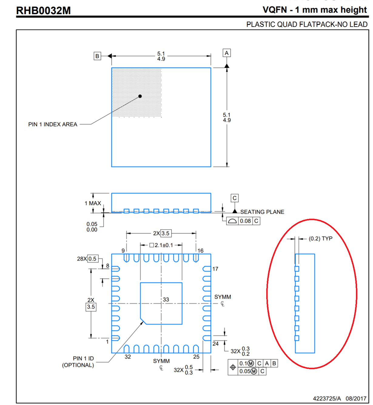
    The thickness of the center pad equates to the thickness of the lead frame.  As shown in the ADS124S08 datasheet the lead frame thickness is typically 0.2mm.

    Best regards,

    Bob B

  • Understood. Thanks!

    -Darren

  • Hi Darren,

    I'm not sure what actually is the concern here.  The QFN package requires the center pad soldered for stability of the package regardless of the pad being used as a thermal pad.  Not all devices require the pad to be used for thermal reasons, which is the case for the ADS124S08.  However, the center pad must be soldered for package stability to prevent package damage when thermal cycling.

    Best regards,

    Bob B

  • Hi Bob,

    I'm sorry, I misunderstood the customer's concern as well.

    In a typical QFN assembly operation, the package body of an individual device is singulated and separated from a “brick” by a sawing operation, which leaves an exposed copper sidewall for each termination. Since this exposed copper does not have any plating, the copper oxidizes. When the device is soldered onto a circuit board, these sidewall areas do not solder consistently. Wettable flank plating is an additional process step which puts a 100% tin plate, with the normal tin plating thickness, on the package underside terminals and an exposed flank. The wettable flank plating is protective of the copper and allows soldering to occur on this external flank area such that optical inspection can be made verifying a good solder fillet joint, and thus a good electrical connection.

    The question was: what is the thickness of this 100% tin (Sn) flank plating on the pins (thermal pad specifically)

    The 3D image of the VQFN package and this document on QFN packages (https://www.ti.com/pdfs/logic/qfnqa2.pdf) indicate there is some form of tin plating on these packages. The customer wants to know the thickness (probably no more than several um ~ several 10s of um)

    Thanks,

    Darren

  • Hi Darren,

    Not all QFN packages are the same.  Almost all QFN packages that I'm aware of in PADC are standard QFN packages that do not have wettable flanks and have a standard finish of NiPdAu (Nickel-Palladium-Gold).  The ADS124S08 uses a standard QFN type package.  The solder is not edge connected but rather soldered along the bottom pad.

    Wettable flanks are most often used with automotive devices.  The package type that I have always seen used with precision ADCs is similar to the package used for ADS1235-Q1.  This package type has the entire surface plated in a uniform way.  

    The package you are referring to is a power device such as the LM53600-Q1.  The package uses a notch through the package edges and then replated.  This is a matte-tin package and seldom used with TI devices.  This package type does not apply to the ADS124S08.

    Best regards,

    Bob B

  • Hi Darren,

    I do not have the plating thickness for the QFN package for the ADS124S08 as this plating is done by the specific lead frame manufacturers and not plated by TI.  However, I can give you some general idea of NiPdAu plating thickness.  The Nickel base layer to the copper will be at a minimum of  0.5um and can range up to 2um on some lead frames.  The Palladium layer will be at a minimum of 0.02um and can range to 0.1um on some lead frames.  The gold finish layer can range from 3nm to 15nm.  The plating will be the same for the center pads as well as the input/output pads around the edges of the lead frame.

    To find the specific composition we would need to find out the specific lead frame vendor and their specifications from the quality team.

    Best regards,

    Bob B 

  • Hi Ben,

    Thanks for the answers!
    I don't need further clarification of the NiPdAu plating thicknesses.

    I do have some follow-up questions on how the ADS124S08IRHBR(VQFN) and ADS124S08IPBSR(TQFP) packages are plated though.

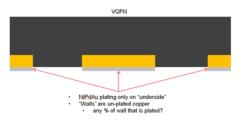
    1. The VQFN package has NiPdAu plating on the underside of each pin, but the "walls" are not plated, correct?
    https://www.ti.com/lit/ml/mpqf130d/mpqf130d.pdf - The "walls" are orange = copper (no NiPdAu), and the "underside" is silver = NiPdAu

    2. Is the non-plated section the entire wall, or just a portion of it?


    3. For the TQFP package, there are leads extending out from the package. How are these leads plated? I assume the plating covers 100% of the lead? If it doesn't, could you help clarify how much of the leg is plated, and where the plating is on the lead?

    If any of these questions require communication with the package group, I would appreciate it if you could help put me in touch.

    Regards,

    Darren

  • Hi Darren,

    For the ADS124S08 devices the plating is NiPdAu.  My understanding is that the NiPdAu finish is applied by the lead frame manufacturer as a pre-plated finish (PMF) as compared to post-mold finish (PMF) used in tin finishes.

    See my remaining responses below.

    Best regards,

    Bob B

    Darren (FAE) said:

    Hi Ben,

    Thanks for the answers!
    I don't need further clarification of the NiPdAu plating thicknesses.

    I do have some follow-up questions on how the ADS124S08IRHBR(VQFN) and ADS124S08IPBSR(TQFP) packages are plated though.

    1. The VQFN package has NiPdAu plating on the underside of each pin, but the "walls" are not plated, correct?
    https://www.ti.com/lit/ml/mpqf130d/mpqf130d.pdf - The "walls" are orange = copper (no NiPdAu), and the "underside" is silver = NiPdAu 
    [Bob] I think here you are referring to the appearance of the simulated package drawing.  With the standard QFN package, the sides are bare copper as the lead frame is cut with a saw leaving the copper exposed.  The rest of the lead frame is plated, whether exposed on not exposed.  

    2. Is the non-plated section the entire wall, or just a portion of it?


    [Bob] As I just said above, the side, or walls as you have stated, are copper with no side plating due to the sawing of the lead frame.  The solder will adhere the pins and center pad to the PCB at the bottom-side.  This is the primary connection and creates stability of the device package.  The solder may or may not adhere to the side walls depending on oxidation of the copper.

    You may find this application note helpful: https://www.ti.com/lit/pdf/SLUA271

    In the application note is the following:


    3. For the TQFP package, there are leads extending out from the package. How are these leads plated? I assume the plating covers 100% of the lead? If it doesn't, could you help clarify how much of the leg is plated, and where the plating is on the lead? [Bob] The lead frame for the TQFP is plated NiPdAu, and similar to the QFN the entire lead frame is plated.  As there is no sawing of the lead frame the entire pin is plated as exposed.

    If any of these questions require communication with the package group, I would appreciate it if you could help put me in touch.

    Regards,

    Darren