This thread has been locked.

If you have a related question, please click the "Ask a related question" button in the top right corner. The newly created question will be automatically linked to this question.

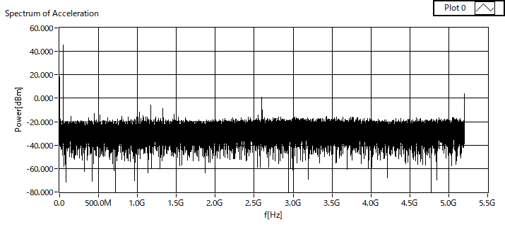
ADC12DJ5200RF: Is there a way to eliminate the 2.6 GHz noise component?

Part Number: ADC12DJ5200RF

Hi,

I use an ADC12DJ5200RF on a board I designed.


A 5200 MHz clock and a 32.5 MHz SYSREF are fed into the ADC, which operates with single-channel 10.4 G sampling.
It seems like the output data has a 2.6 GHz noise component that should not be present. Is there a calibration method to reduce this?
The current settings and waveform FFT results are attached below.

Address(Hex) Set
0x0 0xb0
0x02b 0x15
0x2a2 0x30
0x200 0x00
0x61 0x00
0x201 0x01
0x202 0x03
0x204 0x03
0x48 0x03
0x360 0x10
0x361 0x10
0x362 0x10
0x363 0x10
0x364 0x10
0x365 0x10
0x366 0x10
0x367 0x10
0x29 0x20
0x29 0x70
0x30 0x00
0x31 0x20
0x32 0x00
0x33 0x20
0x60 0x01
0x61 0x00
0x62 0x05
0x61 0x01
0x200 0x01
0x2b0 0x01
0x6c 0x00
0x6c 0x01

  • You are seeing the interleaving spur at Fs/4.  This spur is expected. Check out the datasheet  spec tables for the expected level.  The interleaving spur is calibrated/minimized according to section 7.4.7 in either background or foreground calibration.  There is also an opportunity to further adjust specific parameters per section 7.4.9 if finer adjustments are needed per your specific use case.

    --RJH

  • Hi,

    Thank you for an answer.
    We will continue to evaluate and make additional adjustments if necessary.

    Is this spar expected because the interleaving spar of fs/4 is caused by the switching of BANK 0/1?

  • Hi,

    This is because there are two channels within the ADC itself that are being interleaved in this mode, therefore this is basically a by-product of offset mismatch between two converter channels.

    Regards,

    Rob