This thread has been locked.

If you have a related question, please click the "Ask a related question" button in the top right corner. The newly created question will be automatically linked to this question.

ADS8681: Configuration Issues

Part Number: ADS8681
I am facing an issue with the ADC ADS8681. 
 
In our Design, SPI port of ADS8681 is interfaced to PowerPC Controller MPC5553.
 
It is observed that, on Power ON, ADS8681 is getting into the default configuration and we are not able to change the settings.  By just issuing the NOP operations, we are getting the SDO output i.e Converted Analog Input value.
Attached is the image of the Timing waveforms captured using Logic Analyser.
 
The Steps & values loaded for ADC configuration is as follows:
 

Sl. No.

Functions

Access Type

Value in Hex

Description

1

Reset Pwr Cntrl Register

Write

0XD005 0069h


0xD204 0000h

0xD404 6930h

First, write 0x69 to Address 0x05 (‘0’ is added at MSB to form 9 bit address)


Reset Register – MSB Data

Reset Register – LSB Data

2

SDI Control Register

Write

0XD208 0000h


0XD408 0000h

MSB Data


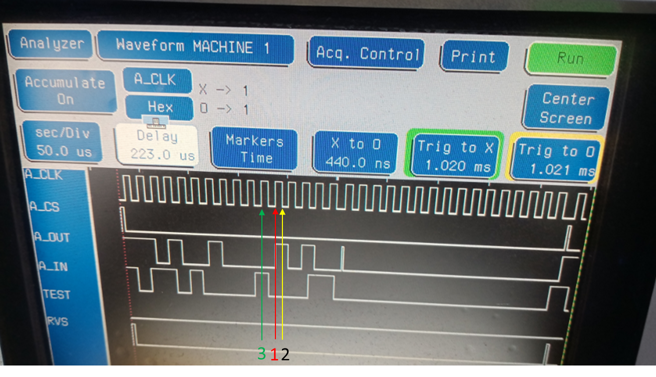
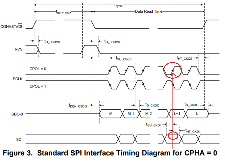
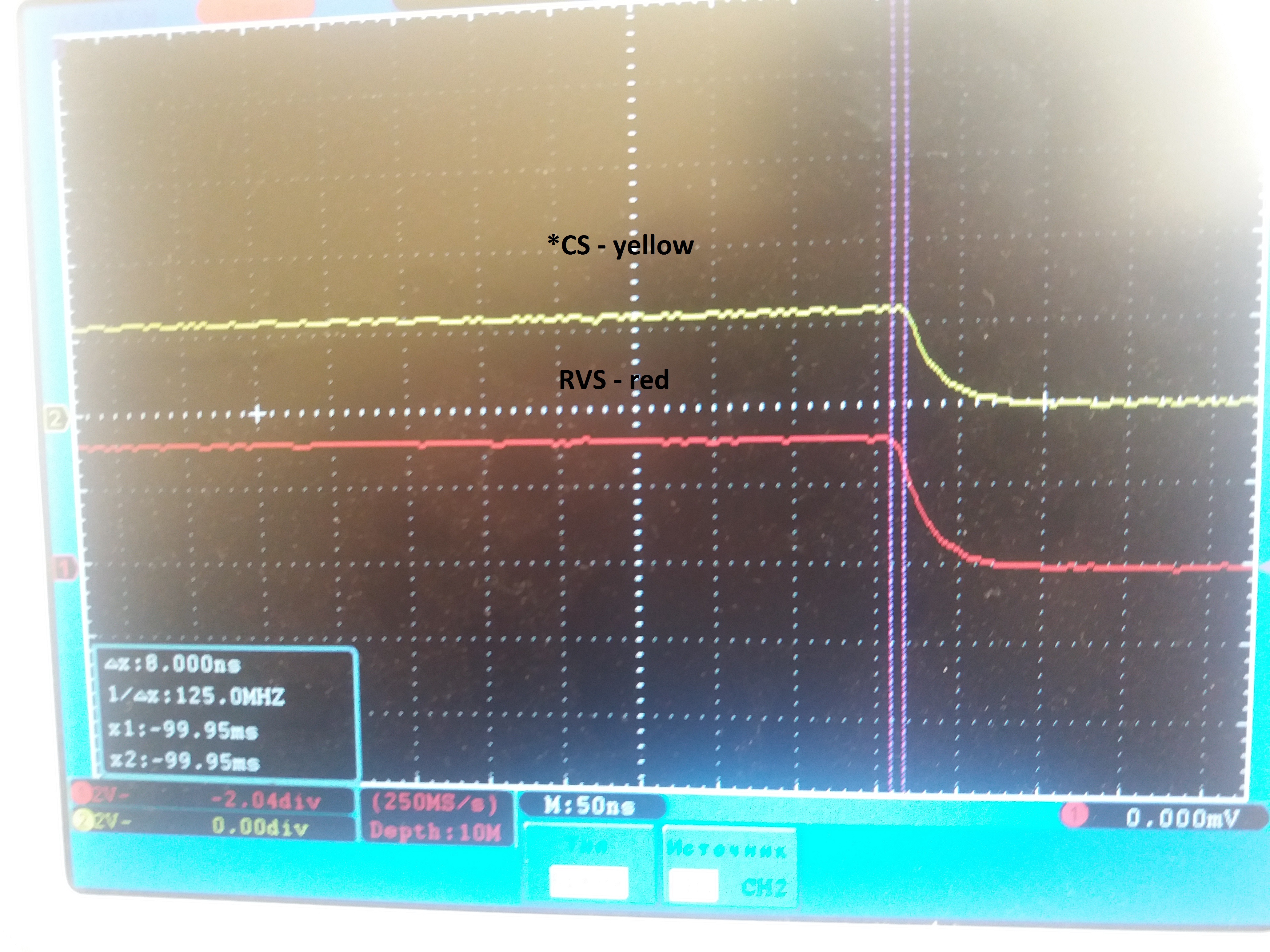
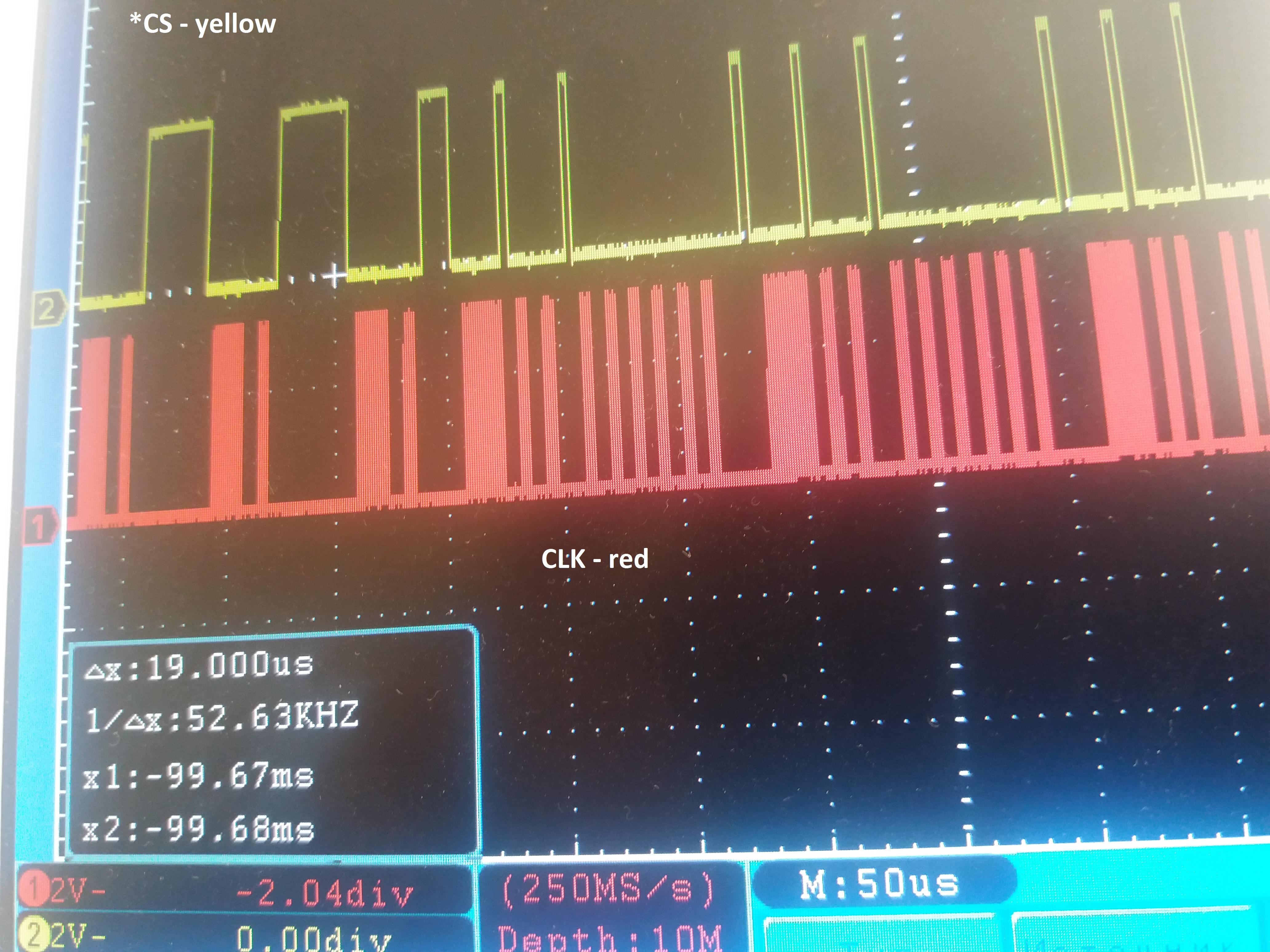
LSB Data – SPI with CPOL=0 & CPHASE=0 (device to Tx data on Rising Edge and Rx Data on Falling edge of SCLK)

3

SDO Control Register

Write

0XD20C 0000h


0XD40C 0000h

MSB Data


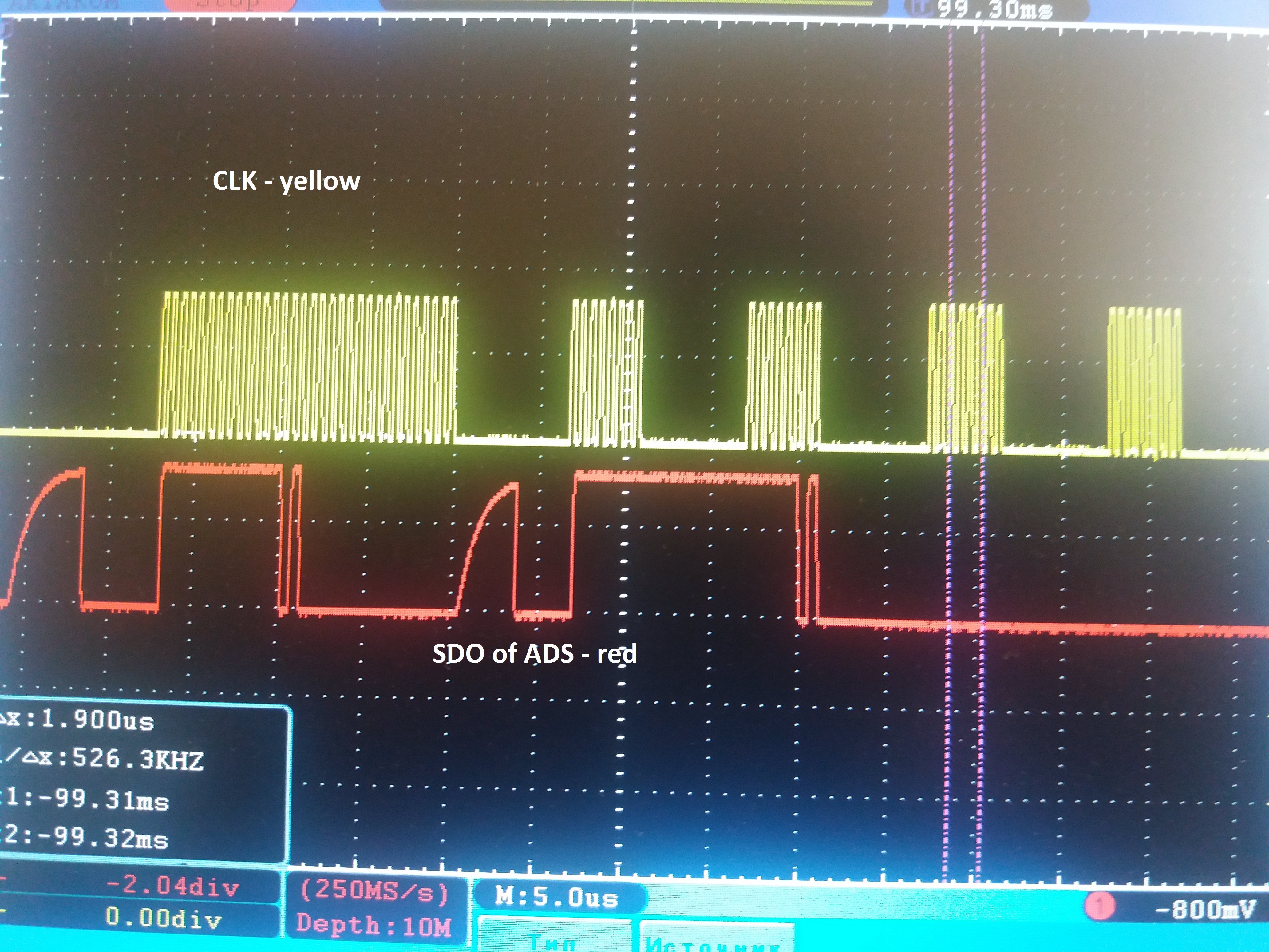
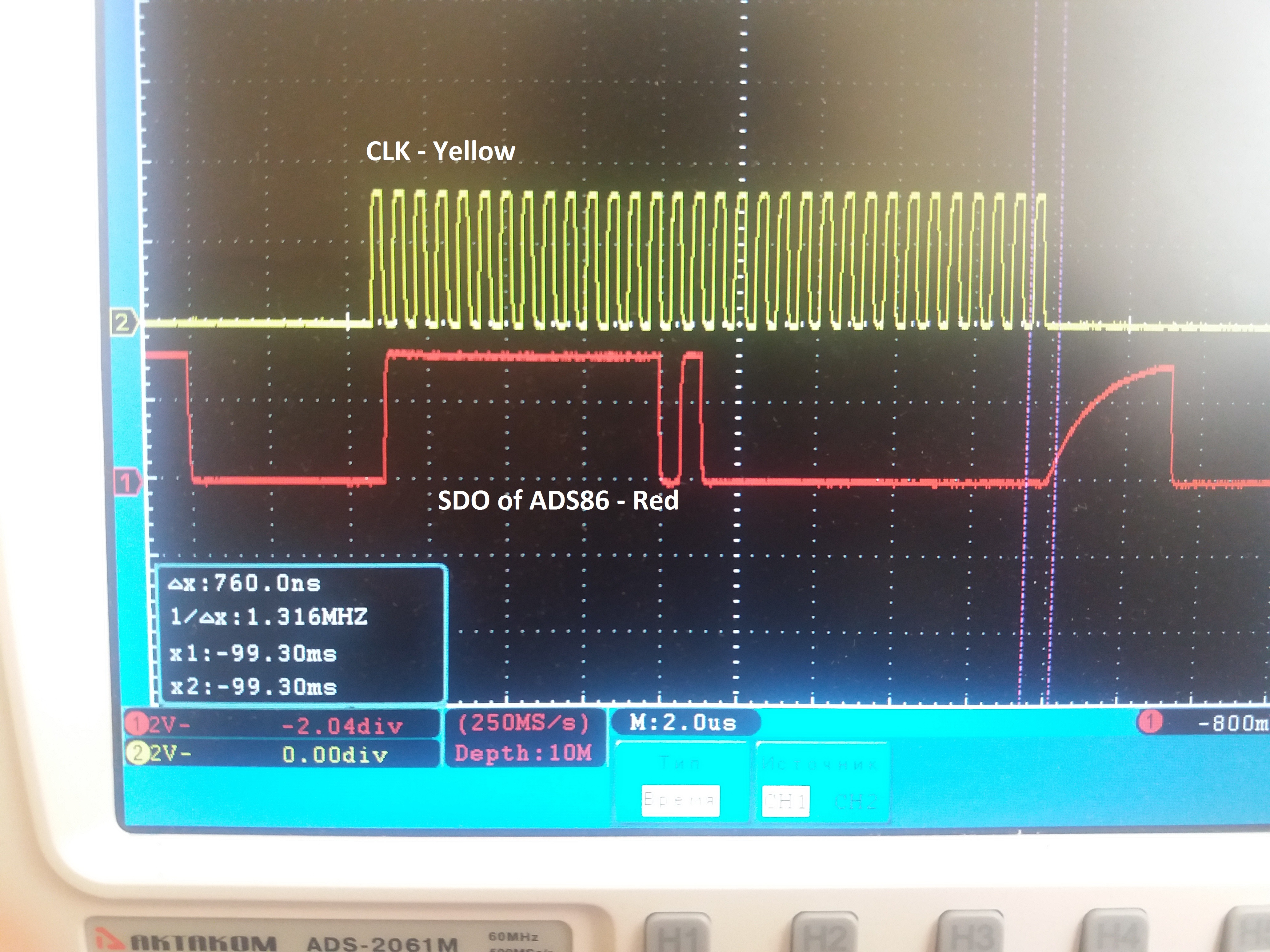
LSB Data – Internal Clock, SPI protocol same as SDI

4

Range Select Register

Write

0XD214 0000h


0XD414 0001h

MSB Data


LSB Data – Internal Ref Enabled, ±10.24V

5

Output Data Control Register

Write

0XD210 0000h


0XD410 0000h

MSB Data


LSB Data – ALARM not included, SDO data does not include Register Address

6

NOP

Write

0x0000 0000h

No operation

In spite of doing the above Register setting, ADC is not changing configuration updates.   We tried giving the Read Command to read the ADC Register, even this operation is not working.
It is reading 0xA1D6 for 3.3V input,  0xB460 for 5V input, 0x7FFC for 0V.
 
When we measure the voltage at ADC Analog input pin, it measures correct set voltage.
 
On the hardware end, we have interfaced SPI_PCS of the PowerPC Controller to CONV/CS_N pin of ADC.   Is there any issue in interfacing the CS_N of SPI to CONV/CS_N pin?
Further, Schematic sheet of ADC is attached for reference.
 
Kindly guide us in changing the configuration settings of ADC.
 
Regards,
 

Poornalatha K

 
  • Hi Poornalatha,

    Firstly, your command for register writing is incorrect, for instance, you are trying to use 0xD0050069 command with 0x05 address to program WKEY on 15-8 bits of RST_PWRCTL_REG register, actually your 69h data was written to the 7-0 bits not 15-8 bits of this register because "LSB of the 9-bit register address is always ignored and considered as 0b"  which is stated in the command table 5. Hence, the next register writing operations were not successful because the WKEY writing was incorrect. The right command should be 0xD2046900 (or 0xD0046900).

    For test and debug purpose, please only write one register then read back the register content to check if your register writing is correct, for instance, only change input range in the RANGE_SEL_REG register. Also, it is easy to check whether your register writing is successful or not, just check the conversion code before and after register programming. Here is an example when the analog input to the ADC is a DC 4V:

    • For +/-1.25Vref (+/-5.12V range), you should get codes around 58340 (decimal).
    • For +/-3Vref (+/-12.88V range), you should get codes around 43425 (decimal).

    Your schematic was not uploaded successfully, please try again.

    I'm not familiar with the SPI of PowerPc controller, it's okay to use the /CS of a standard SPI bus for the /CS of this ADC, however notice that the /CS pin on the ADS8681 is a dual-functionality pin, the rising edge of the signal on this pin will initiate a data conversion and bring the device from the acquisition phase to the conversion phase, thus any jitter on this signal will affect the performance in your system.

    Best regards,

    Dale

  • Sir,

    I tried again, but still I am not able to change the value of Range selection Register.

    The ADC portion of Schematics is as follows:

    Sequence of command given is as follows:

    1. Range SEL (MSB): 0xD214 0000
     
    2. Range SEL (LSB): 0xD414 0001
     
    3. RD : 0xC814 0000
     
    4. NOP command : 0x00000000
    The Logic Analyser Timing waveforms are as follows:
    2.  Range SEL (LSB): 0xD414 0001
     3.  Read Command (Address 0x14) : 0xC814 0000

    4. NOP command : 0x00000000

    Regards,

    Poornalatha

  • Hi Poornalatha,

    I did not see any schematic or timing plots you uploaded, please check. Also,

    1. A closer timing plot for each command will be helpful.

    2. Let me know you analog input signal and the output code before and after programming the register.

    3. Please check if a 4.096V can be measured on the REFIO and REFCAP pin.

    Regards,

    Dale

  • Sir,

    1.  I am trying to share the Schematics and Logic Analyser waveforms captured by pasting the images. After sending the Reply, images are turning into small boxes.  Let me know the way to share the images.

    2.  We are feeding a fixed voltage of 5V at Analog Input. On applying the NOP command itself, we are getting the output code as 0xB42E.  After programming the Registers also, the output Data is same.  If we feed Analog Input voltage as 3.3V, Output code with NOP command on Power ON, is 0xA430.  Device is not responding to any of the Register setting.

    3.  Measured Voltage on REFIO  is  4.090V and  REFCAP is  4.090V.

    Regards,

    PoornalathaRange SEL (MSB).pdfRD.pdf

    .

  • Hi Poornalatha,

    The timing in pdf file works, thanks.

    I hope you configured your SPI interface to mode 0 (CPHA=0 and CPOL=0) on your controller, your controller is expected to launch the data out at the falling edge of SCLK so that the ADC can capture it at the rising edge. However, your timing looks opposite, please see you timing for register writing below. I believe the "A_OUT" is the MOSI signal from your controller to the ADC which is the SDI for the ADC and also the "A_IN" is the MISO signal from the ADC(SDO) to the controller.

    If we look at the data on the "A_OUT" (MOSI), the data was launched at the rising edge of SCLK (red arrow on position 1), the best position to capture it in this timing is the position 2 yellow arrow which actually is the falling edge of the SCLK, however the ADC always captures the data at the rising edge of SCLK according to the mode 0 in the datasheet. This situation leads to an incorrect data capturing for the device. By the way, the data from the controller on the "A_OUT" shows 0xD2140000, actually this command with all 0s data does not change any bit (bit 15-8) in the RANGE_SEL_REG register, however I believe you sent one more command 0xD4140001 regarding your procedure which can change the input range to +/-2.5Vref in the same register.

    If we look at the data on the "A_IN"(MISO) which is the data output from the ADC, they were launched at each falling edge of SCLK and this is a correct operation so that your controller can capture it at the rising edge of the SCLK (green arrow on the position 3 which is also the centre of the data).

    The same behavior happened in your timing of register reading. Hence, please check the configuration on your controller. The 2nd timing below shows the edge of SCLK in red expected by the ADC in the datasheet.

    Also, I would suggest you:

    • Add a delay between the falling edge of /CS and the first SCLK. Right now, it's too close and the first SCLK pulse may be ignored.
    • There is a very narrow high pulse on the "A_OUT" which may indicate that the first 16 SCLK clocks are ended. This is a potential risk for incorrect data reading. Please check and try to eliminate it.

    The data you got after power-on are correct for default +/-3Vref input range.

    Best regards,

    Dale

  • Sir,

    Controller is configured to CPOL=0 and the CPHA=1 (as per the controller datasheet) i.e. controller launch the data out at the Rising Edge of SCLK, So that ADC can capture it at the Falling edge.

    Similarly, on ADC, the registers are configured to CPOL=0 and CPHA=0 (as per the datasheet) i.e. ADC launch the data out at the Rising Edge of SCLK, So that Controller can capture it at the Falling edge.

    The Signal referred as ‘A_OUT’ is MOSI and ‘A_IN” is MISO.

    Herewith I attaching the waveforms for the command 0xD414001  and Read command3683.RD.pdf

    We will try to increase the gap between the CS going low and the Rising edge of SCLK.

    Regarding, the small pulse, we will try to clear it. As the controller is configured for 16 bit data, it is putting out 2 cycles to meet the 32bit ADC requirement.

    The continuation of  CS for 2 cycles, gives the pulse after the 16bit. 

    Regards,

    PoornalathaRange SEL (LSB).pdf

  • Hi Poornalatha,

    Firstly, your understanding about  CPOL=0 and CPHA= 0 (mode 0) on the ADC is incorrect. In mode 0, the  ADC will launch the data out at the falling edge of SCLK, and the controller is expected capture the data at the rising edge of SCLK under mode 0, also the ADC will capture the data on the MOSI at the rising edge, not the falling edge as you expected.

    Secondly, when the ADC is configured to the mode 0 (CPOL=0 and CPHA= 0), the controller must be configured to the same  mode (CPOL=0 and CPHA= 0), thus  the timing for both ADC and controller can match well.  This is the reason why you could not successfully program the internal registers of ADC. 

    Regarding the small pulse, it's not the reason to cause the issue, however it's good to see a clean timing since it's not shown on /CS.

    Best regards,

    Dale


  • Sir,

    With the above said suggestions, we were able to configure ADC and the read the Digital Data.  

    Thankyou very much.

    Regards,

    Poornalatha

  • Hello, Sir!

    I have faced almost with the same problem which was mentioned in above disscussion. Little bit tired to struggling with this issue.

    I attached here the some code with working ADS8681 and some pictures from oscilloscope. Could you help me, Sir?

    As you see the Fclk of SPI is almost 2 MHz.

    And here the codes:

    The receiving data about samples value is OK. But except of that i couldn't get nothing, i couldn't get the values from command registers. How to do it properly?

    Also, you suggested that the mode of SPI should be configurated to 0, both - ADC and microcontroller. I have executed it. Thank you!

  • Sir, I found some mistakes on mine words and get started to fix that sentences, but with clicking "edit" in my smartphone I have ruined some detailed information about issues. I mean I lost some attached pictures. Sorry, I will rewrite this questions again tomorrow on my PC. 

    Already rewritten and the message has been corrected.

  • Hi Osim,

    Your timing graphs really confused me. I do not need a timing covering so many frames which is difficult to check the data. I only need your a timing for register writing if you did, also the timing for register reading command and next frame to shift the register data, these timings should include /SCLK,SDI, SDO and CONVST/CS signals. Please refer the timing Poornalatha captured and shared which are clear for me to check. Also, please open a new thread since this thread has bee closed. Thanks.

    Best regards,

    Dale