


Part Number: ADS8681
Hello Forum,
I'm trying to establish a SPI connetcion to the programmable analog digital converter TI ADS8681. In the future I wish to adress several ADCs connected in a daisy chain (see ADC data sheet p.38). But as a first step I set up a connection to a single ADC, according to figure 71 (ADC data sheet p.37). I connected a "aa battery" to the ADC to simulate an input. The ADCs digital output shall be send via SPI to an Arduino MKR 1010 Wifi via SPI. The Arduino forwards the signal to the serial port of a PC. My wiring is shown in the picture.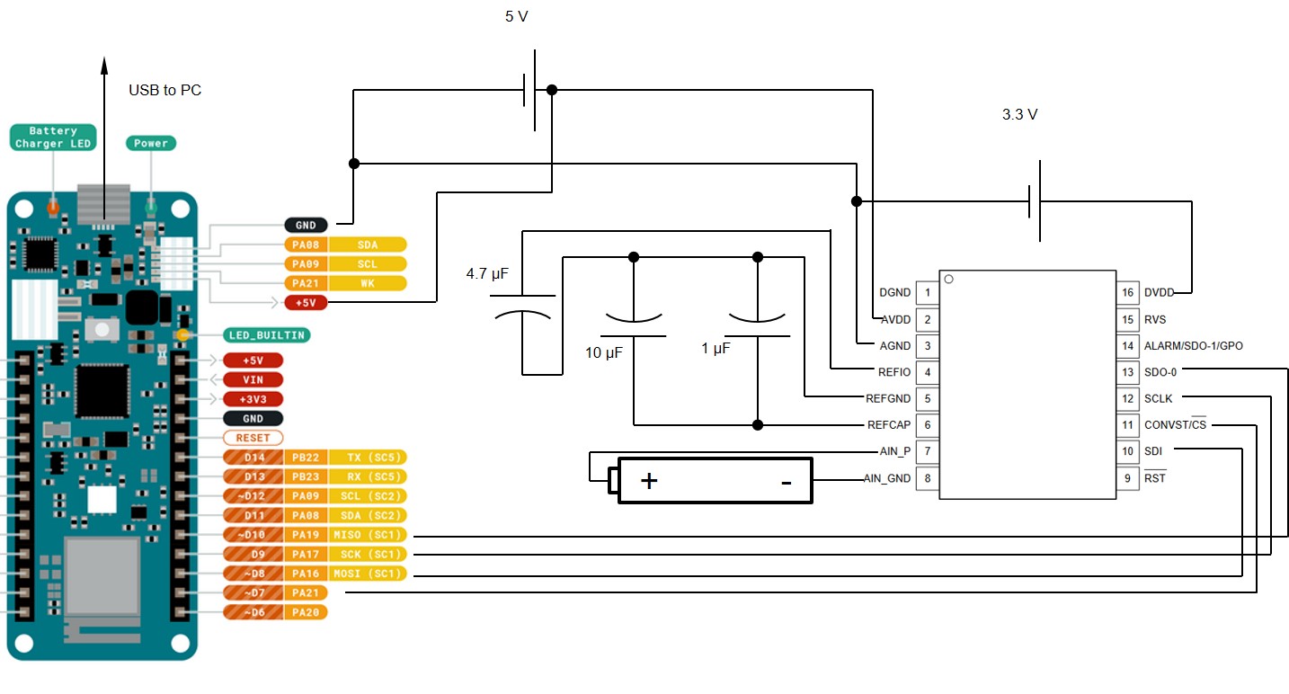
I wrote a code (at the end of the post) to configure the ADC via its command registers and read the converted digital values. But the 16 bit device only returns 65635. With the measurement range of +-10,24 V and a battery voltage of ~1,5 V something isn't working the way I want it to do.
I suspect the configuration of the ADC isn't working and he is in the mode 101b for the DATA_VAL[2:0] of the DATA_OUT_CTL_REG Register only returning ones.But I don't get where the error is.
I would be rateful for any advice how to recieve suitable data.
// Read out a TI ADS8681 (ADC) with a Arduino MKR 1010 WIFI
// August 2020
// by SPL
#include <SPI.h>
// Arduino SPI libray
// MISO, SCK & MOSI are defined by the library
const int CS = 7;
// set SPI Pins
void setup() {
Serial.begin(9600);
// define Baud rate for serial data transfer
pinMode(MISO, INPUT);
pinMode(MOSI,OUTPUT);
pinMode(SCK, OUTPUT);
pinMode(CS, OUTPUT);
// set the SPI-Pin as an output/input:
digitalWrite(CS, HIGH);
SPI.begin();
// start SPI and set CS to idle
SPI.beginTransaction(SPISettings(100, MSBFIRST, SPI_MODE0));
// initialize SPI & SPI Settings defines speed Maximum in Hz, dataOrder and dataMode
// speed Maximum 67 MHz, ADW Data Sheet p. 11, MSBFIRST, ADC Data Sheet p. 38, dataMode ADC Data Sheet p. 45;
writeRegister(0x08,0b00000000, 0b00000000);
// define SPI Mode; address of the SDI_CTL_REG Register (hex) and define SPI Mode, ADC data sheet p. 51, matches ARDUINO SPI Mode0
writeRegister(0x10,0b00000000, 0b00000000);
// define DATA_OUT_CTL_REG;
writeRegister(0x14,0b00000000, 0b000000000);
// define Measurement Range +-10,24 V, see p. 54 ADC data sheet;
}
void loop() {
read_adc_to_serial();
//read ADC and send result to serial
}
void read_adc_to_serial() {
byte dataFrame [4];
// initialise
digitalWrite(CS, LOW);
// CS low to start data transfer
SPI.transfer(dataFrame,4);
// read shift register in variable 'dataFrame';
digitalWrite(CS, HIGH);
// CS high to stop data transfer
word package_read = dataFrame[0]<<8 | dataFrame[1];
Serial.println(package_read, DEC);
// convert and print out data to serial;
delay(1);
// delay t_cycle-min for ADS8681, p. 665 & 11 ADC data sheet
}
void writeRegister(byte thisRegister, byte thisValue1, byte thisValue2) {
// see ADC programming p.43 data sheet
byte package [4] = {0b11010000,thisRegister,thisValue1,thisValue2};
// opcode, see p. 43 ADC data sheet
digitalWrite(CS, LOW);
// take the chip select low to select the device:
SPI.transfer(package,4);
//Send register location & value
digitalWrite(CS, HIGH);
// set chip select high to de-select
}
