This thread has been locked.

If you have a related question, please click the "Ask a related question" button in the top right corner. The newly created question will be automatically linked to this question.

ADS131A02: Register output data are all 0x2272

Part Number: ADS131A02

Hello,I have encountered a problem, that is, I bought an ADS131A02 chip a few days ago, and now I have configured the driver to output 0x2272 data when reading each register. When reading the data output of 32-bit AD, it is found that the data output is 0x00002272. Now I don't know what the problem is and how to solve it.

  • Hi,


    The ADS131A02 is very specific about how the communications should be and what it expects for the command words. My guess is that there's something wrong with the communication frame and that the response you are getting is a STATUS response because the device does not understand the command. Note that the first part of the STATUS response is 22h, which is the equivalent of a READ of the 2h register (which is STATUS).

    First, what are your settings for the M0, M1, and M2 pins? and are you using dynamic frame mode of fixed frame mode for communication? Please note that for any mode of communication, you should complete you communication, and give enough SCLK pulses.

    It may also help to show the SPI communication with the device. You should get an oscilloscope to show the DIN, DOUT, CS, and SCLK to show what the device is sending and receiving. Once you are able to view the communication, you can post it back here. It may also be helpful to explain what command sequences you are sending to the device and the timing between them. Note that the command responses are also helpful, as they can be used to debug the commands sent from the previous frame.


    Joseph Wu

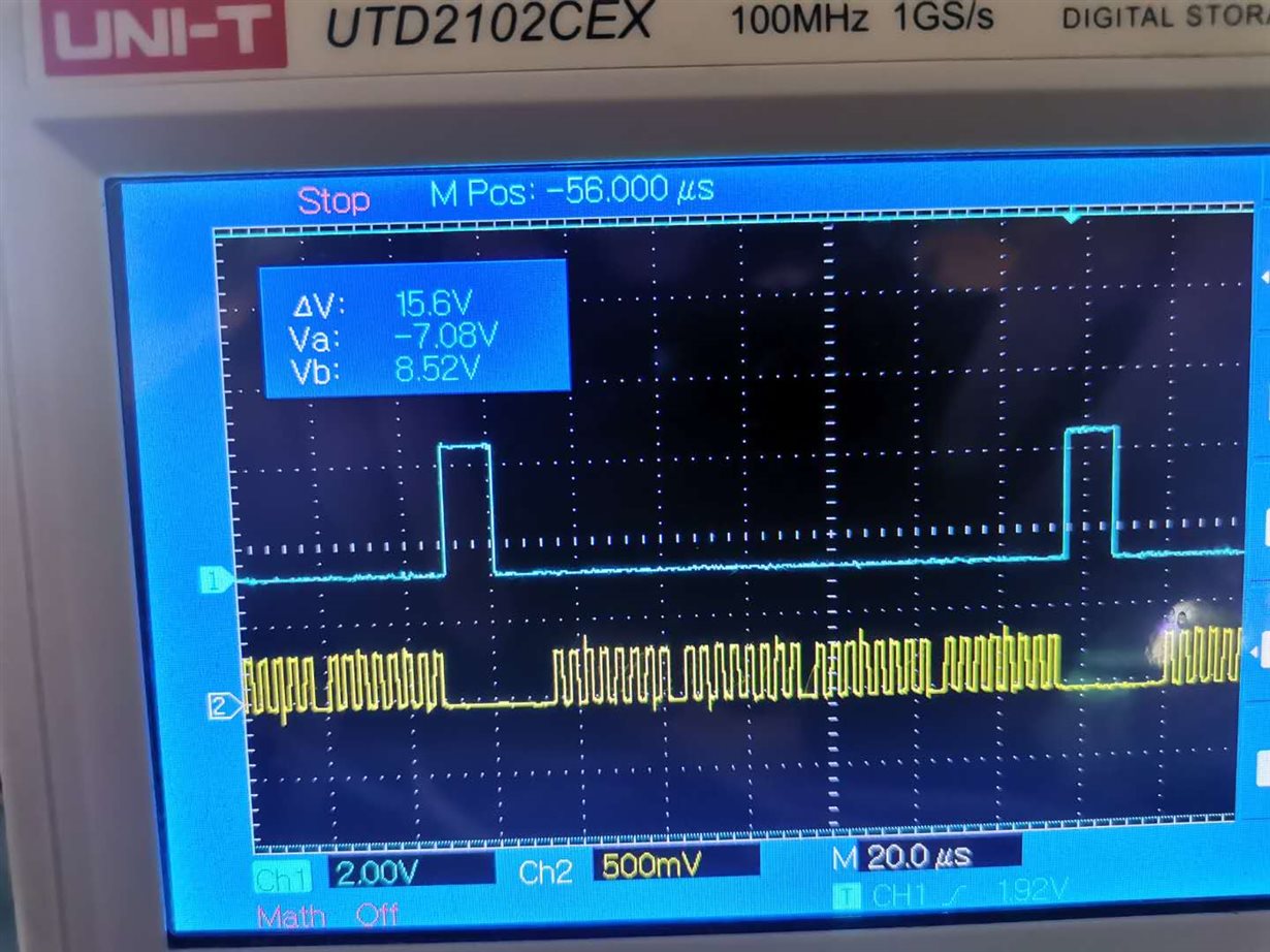
  • I use an oscilloscope to measure the waveform of CS,SCLK,:1 is CS,2 is SCLK. and the results are as follows:

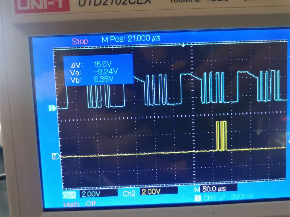
  • I use an oscilloscope to measure MISO and MOSI, and the results are as follows:1 is MISO,2 is MOSI.

  • My SPI frequency is 72 MHz ,256 frequency division,Then CLK1 is set to 0x80,CLK2 is set to 0x2F .M0= VDD , M1=GND.

  • Hi,


    Again, what settings are you using for the device? I asked several questions about the M0-M2 setup and the frame modes that you are using in my last post.

    The problem that I see in your scope shots is that the /CS line returns high every 32 SCLKs. If you are using the ADS131A02 with 32 bit words, and if you're using Fixed Frame mode (I'm just using this as an example). Then your communication will be 4 data words long. The communication would be the STATUS word, the Channel 1 data word, the Channel 2 data word, and then the CRC word (which would be all 0s if CRC is disabled).

    In operation, /CS goes low to enable the communication, then you transmit all four words. This is a total of 32x4 (or 128) SCLKs and then /CS goes high. You cannot break up the communication into 32 SCLKs for each /CS active period.

    Change your communication to send 128 SCLKs for each communication and see what you get.


    Joseph Wu

  • Hello, the communication is normal now, but when I read the 03 and 04 registers, it prompts me to exceed the range, but now my input is grounded and also prompts me to exceed the range. What is the problem?

  • Hi,

    I assume that you are looking at the STAT_P and STAT_N registers and seeing the inputs have exceeded the values for the threshold detect. What is the reading of registers 03h and 04h?

    Also, what are your input values set to? What is your voltage for AVDD and for AVSS? Do you have the negative charge pump enabled? 

    If you have AVDD=3.3V and AVSS=0V, and the negative charge pump is off, then connecting your negative input is going to be below the threshold voltage.

    However, if you have the negative charge pump on, the AVSS=0 is a in the range of input and not exceeding the threshold.

    Read through my questions carefully and send me your answers.


    Joseph Wu

  • I'm sorry, maybe I didn't make myself clear. When I read the STAT_P and STAT_N registers, the data they returned were: 0x2303 and 0x2403. It is suggested that my IN1 and IN2 positive input and negative input both exceed the threshold.However, my IN1 and IN2 have both positive and negative inputs of 0. My input settings are as follows: AVDD=5v,AVSS=0V,IOVDD=3.3V, enables the negative charge pump.

  • Hi,


    First, with the negative charge pump enabled, your AVDD to AVSS can be a maximum of 3.6V. Only when the negative charge pump is disabled, can the AVDD to DVDD be 5V. This comes from the Absolute Maximum table which you can see below.

    Also, with the negative charge pump enabled, the device recommended operating range is from 3.0V to 3.45V. This comes from the Recommended Operating Conditions table in the datasheet.

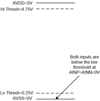
    Now, if you have run the supply from 0V to 5V, then it is likely that the negative charge pump is not working correctly. I would guess that the supplies are still at 0V and 5V. If you haven't changed the threshold settings, then the threshold settings of COMP_TH in the A_SYS_CFG register are still set to 95% of the supply for the high threshold and 5% of the supply for the low threshold.

    Then, if the inputs are at 0V, then both inputs are below the low threshold:

    This will cause the flags for both 03h and 04h to be set. I think this is the likely cause of the problem. If you can, change the inputs to be near mid-supply to see if the flag goes away. Or you can change the supply to 3.3V and then enable the negative charge pump. I would also note that there is a chance that the device is damaged with the supply at 5V with the negative charge pump. However, I haven't heard of cases of damage from a device accidentally being put in this mode.


    Joseph Wu