This thread has been locked.

If you have a related question, please click the "Ask a related question" button in the top right corner. The newly created question will be automatically linked to this question.

ADS1263: Reference Circuit dan Biasing Resistor for Floating Input from 4-20mA Sensor

Part Number: ADS1263

Hello, my name is Bontor from Tritronik, Indonesia. We are designing an IoT device (datalogger) that needs to read 10x sensors with 4-20mA output. Since all sensors and datalogger will be installed in a noisy outdoor environment, we need to take safety precaution in this design. We feel ADS1263 is suitable for this application since it has sufficient number of channels, sampling rate, and especially with TIDUC03 - "4- to 20-mA Analog Input Module Reference Design for Safety Applications" recommending such ADC chip for 4..20mA application.

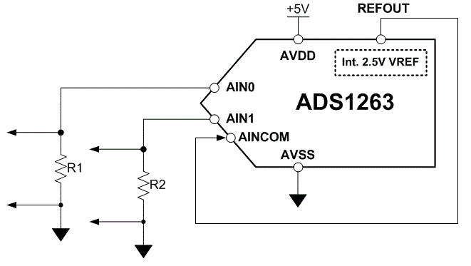
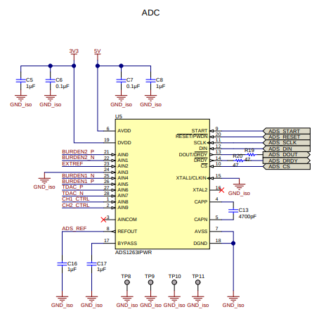
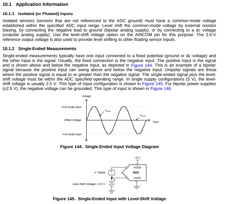
While we can use design references in TIDUC03 document, it doesnt show how to design a circuit for floating / single channel 4..20 mA application. Nor we find such design in ADS1263 datasheet. Closest we can get is as shown below from ADS1263 datasheet page 107

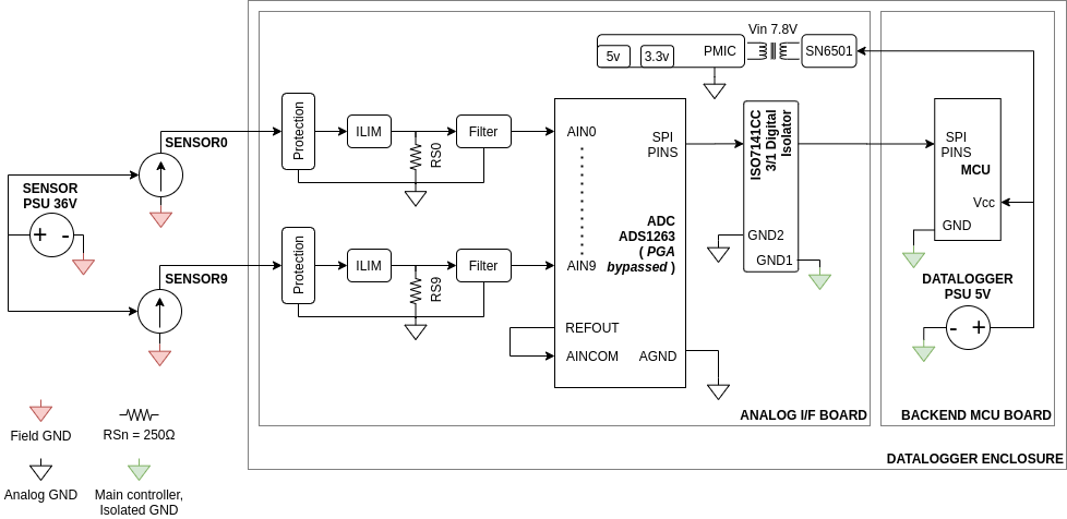
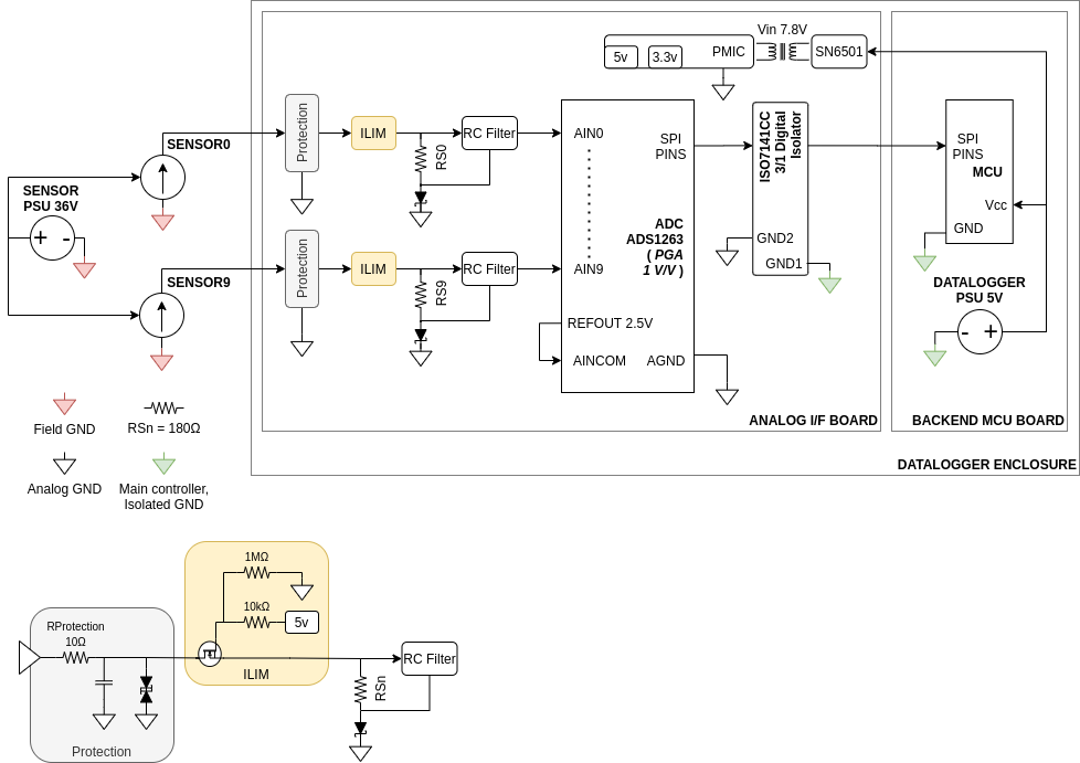
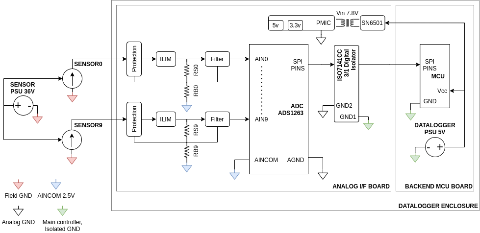
Based on TIDUC03 and Application Information above, we conclude that to use ADS1263 to measure floating input 4..20 mA in a single channel, we need to add external resistor to bias the +/- signal. Which means that the burden resistor, protection circuit (TVS diode), and analog filter in the analog front end should be connected to the bias resistor. We come up with high level design below, where RB0 will bias input signal to the ADS1263

My questions are:

  1. Is my design above, especially the way i interpret "biasing resistor", correct?
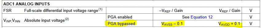
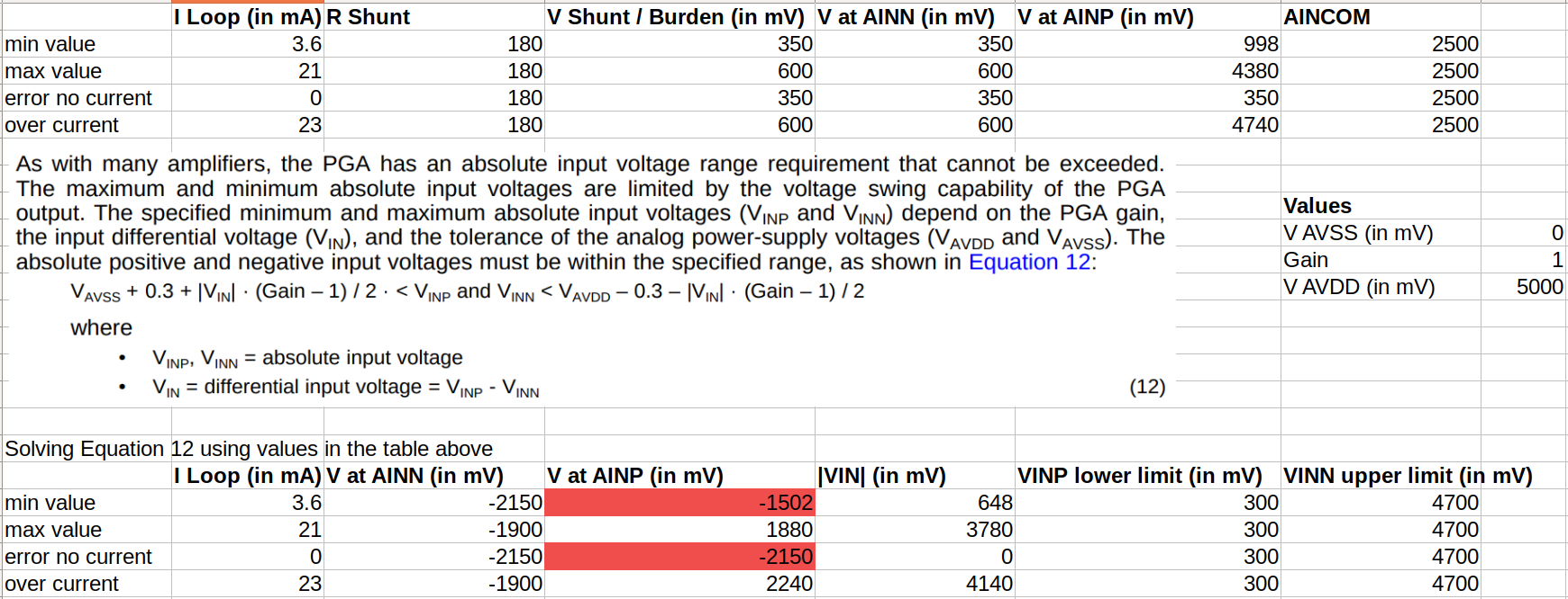
  2. To determine the value for biasing resistor (RBx), i will need to calculate the range of input signal, and ensure that the input signal is within ADC Input Voltage Spec → as mentioned in ADS1263 datasheet pg 116 "The next step in the design is determining the value of the RBIAS resistor, in order to level shift the RTD voltage to meet the ADC absolute input-voltage specification"
  3. Finally, regarding PGA, TIDUC03 recommends to use PGA 1/1 in order to increase input impedance. However, the way I understand it, ADS1263 datasheet page 119 does not specifically explains DO's and DONT's on using PGA for floating input circuit. Can I configure PGA 1/1 with my design above?

Thank you for taking your time reading this post.

BR,

Bontor
www.tritronik.com

  • Hi Bontor,

    Typically the current shunt resistor is ~250ohms, which results in an input voltage range of 1V to 5V for a 4-20mA input. If you bias the bottom of the shunt at 2.5V, then your input range will be 3.5V to 7.5V, which is outside of the allowable input range for the ADC (limited to AVDD).

    Since the ADC in your system is isolated from the backplane, the analog ground will simply float to the field ground potential. Therefore, you should be able to just ground the bottom of the shunt, assuming there is no common-mode voltage difference between the two shunts you are trying to measure. In other words, assuming all of the field sensor grounds are at the same potential.

    To make this type of measurement with the ADS1263, you would need to bypass the PGA to avoid the common-mode limitations of the PGA as shown in the first image below. With the PGA bypassed, you can measure the shunts in two different ways:

    1. You can use the ADC's internal reference as the reference source, and then tie the 2.5V REFOUT pin to AINCOM. Then, if AIN0 was at 20 mA (or 5V), your measurement between AIN0 and AINCOM would be 5V - 2.5V = 2.5V. If AIN1 was at 4 mA (or 1V), your measurement between AIN1 and AINCOM would be 1V - 2.5V = -1.5V. This would allow you to use more of the ADC's full-scale range, and is shown in the second image below
    2. If you want to ground the AINCOM pin and measure against this input, you would need to use an external 5V reference as shown in the third image below. If AIN0 was at 20 mA (or 5V), your measurement between AIN0 and AINCOM would be 5V - 0V = 5V. If AIN1 was at 4 mA (or 1V), your measurement between AIN1 and AINCOM would be 1V - 0V = 1V. So you would only be using the ADC's positive full-scale range in this case

    Again, all of this is predicated on your shunt resistor have a 250ohm impedance. But you could scale these values accordingly if you used a different shunt value.

    Let me know if this makes sense.

    -Bryan

  • Hi Brian, thanks so much for your prompt and clear reply. Based on your suggestion, which btw I agree, i want to clarify and ask one other question

    1. Clarify: as per your suggestion, the new design would be as follow:


    2. Ask: in previous design, I forgot to add the Schottky diode, which is responsible to protect against reverse polarity as per the TI Design Document (https://www.ti.com/lit/ug/tiduc03/tiduc03.pdf page 8). However, since field sensor GND is separated from ADC GND, hence there is zero possibility of reverse connection between 4-20 output and ADC GND, there is no need for Schottky diode in my use case. What is your opinion on this?

    Thanks

  • Hi Bontor,

    Are you talking about the diode in the image below, which is from the TI reference design schematic? If so, this diode is used to lift the common-mode voltage of the analog inputs into the input range of the ADS1263's PGA. It is not for protection.

    In the reference design, they enable the PGA and set the gain to 1 V/V. You could bypass the PGA, but this reduces the input impedance which was important in the reference design. With the PGA enabled, there are limitations on the input signals to the ADC, which is ~300mV above AVSS. So they are just using the 350mV voltage drop across the diode to provide this voltage.

    Let me know if this makes sense.

    -Bryan

  • Hi Bryan,

    Yes indeed I was talking about diode D2, which according to TI Design Guide pg 8 "Diode D2 prevents an uncontrolled current flow during reverse polarity connection." Although the document previously stated that "Diode D2 lifts AINN to a voltage greater than VAINP/N,MIN at the minimum loop current of 3.6 mA."

    I understand now. Based on your explanation and the statement "For best performance, the input impedance (RADCIN) of the ADC channels is maximized to reduce the voltage drop over the protection resistors put in series in front of the inputs. RADCIN is dependent on the usage of the integrated programmable gain amplifier (PGA)." I think protection resistor is important, hence the need of PGA to increase input impedance. Therefore i need the diode to lift the common mode voltage and Rshunt must be selected to ensure that voltage at AIN0...9 is between 0.3V and 4.7V, since I am using a unipolar 5V supply.

    Does this make sense?

    Thanks.

  • Hi Bontor,

    Yes, I missed the second mention of D2 on page 8, where it talks about reverse current flow. I only saw the first comment about shifting the input common-mode voltage.

    So it looks like D2 serves 2x purposes: shifting the PGA VCM, and protecting against reverse polarity connections (where the user miswires the power supply or otherwise applies a large negative voltage to the inputs). It might be challenging to guarantee that the user of your system would never be able to miswire the power supply, etc., so I would still consider protecting the inputs against these types of faults, even if you choose not to use a diode (and you level-shift the PGA VCM in a different way).

    Since you do not need to measure voltages below ground, a unidirectional TVS diode on the inputs might be sufficient to protect against these types of events. You would just need to ensure that the peak power dissipation specs are met. You can learn more about EOS events and protection circuitry with our Precision Labs content, specifically the modules in Chapter 9.

    But even if you just used a TVS diode, you would still need to level-shift the PGA common-mode, so using D2 might be your best option.

    -Bryan

  • Hi Bryan,

    Thanks for your clarification. So far, I note several important things which are aligned between aforementioned TI documents and your explanations:

    1. In 4-20mA application where protection resistor is needed, we have to use PGA to increase input impedance
    2. Using PGA means that VINP and VINN are limited, according Equation 12 in https://www.ti.com/lit/ds/symlink/ads1263.pdf page 38
    3. In 4-20mA application where we have to add protection against miswiring of power suppy etc, we need to add Schottky Diode (D2) between RShunt and ADC Analog GND. This diode also shift the PGA input to desirable range (which is 300-4700 mV on 1 V/V gain configuration)

    Additionally, I used eq 12 to find value for RShunt:

    Based on the three premises, equation 12 calculation, and the fact that TI Design Guide Schematic below, where AINCOM is left disconnected

    I come up with the following design which should help others who are trying to use ADS1263 with floating input configuration for 4-20 mA application. 

    However I still have a doubt about this design, as it violated DONT'S rule in ADS1263 datasheet, page 19. It doesnt talk about design for floating input circuit, but leaves lingering concern that if we enable PGA and uses unipolar power supply 5V, we need to offset AINN by 2.5V (ie by wiring REFOUT 2.5V to AINCOM). While if we wire AINCOM to REFOUT, this means we offset VINP (V at AINP) and VINN (V at AINN) by 2.5V. thus bringing the values outside PGA input voltage range as shown in table 2 below

    What is your opinion on the new design and the concern about Figure 158 in ADS1263 datasheet?

    Thanks

    BR,

    Bontor

  • Hi Bontor,

    I am glad this is making sense now, and thanks for sharing your block diagram and detailed proposal. I am sure this will be useful for future engineers trying to solve the same problem.

    I am not too sure I understand your concern about Figure 58 however. The way your block diagram is wired is exactly as it is shown in the image below, also from Figure 158. The diode you have should level shift the voltage such that your inputs are within the PGA's common mode range as defined by equation 12. You can see from this equation that when gain = 1, the limits simplify to just AVSS + 0.3V < AINP and AINN < < AVDD - 0.3V.

    AINN will always be in that range since you have REFOUT (2.5V) connected to AINCOM, where AINCOM will be your AINN signal. For AINP, the diode ensures that the lower limit (AVSS + 0.3V = 0.3V, since AVSS = GND) is met, since the diode voltage drop is >0.35V. Your maximum differential voltage applied to the inputs is 23mA*180ohm = 4.14V. This voltage must be added to the diode voltage drop such that the maximum voltage at AINP should be 0.35V + 4.14V = 4.5V. This is still well below your limit of AVDD - 0.3V = 4.7V, since AVDD = 5V

    So I believe your system is setup correctly, please let me know if I missed something.

    -Bryan

  • Hello Brian,

    Thanks a lot, you have cleared my confusion. The key is "AINN will always be in that range since you have REFOUT (2.5V) connected to AINCOM, where AINCOM will be your AINN signal" Previously I thought that applying AINCOM to 2.5V will offset the voltage such that AINP = AIN0 - AINCOM, so when sensor outputs 3.6mA, AIN0 is 0.3V and AINP = 0.3V - 2.5V = -2.2 which is well below AINP lower limit of 0.3V. Please ignore my calculation table number 2, its all wrong.

    Now that I understand it:

    1. AINN must be connected to AINCOM, means setting Input Multiplexer Register (INPMUX) [3:0] to 1010

    2. AINP will be connected to AIN0... AIN9, which by using the schottky diode, will have lower limit of 0.3V. Hence satisfying PGA input range requirement. When the sensor output 23 mA, the voltage at AINP will be 0.35V + 4.14V = 4.5V, again within PGA input range requirement

    Hence this would be the final design

    One final thing, I found out that its easier to use connect VBIAS to AINCOM rather than connecting REFOUT to AINCOM. As shown in ADS1263 datasheet below

    We can just use VBIAS instead of hardwiring REFOUT to AINCOM, right?

    That would be my final question for this design. Thanks

  • Hi Bontor,

    Yes I believe you have it now.

    Keep in mind that Equation 12 is specific to the absolute input voltage on each pin. In other words, the voltage you apply to any of the analog inputs (AIN0 through AIN9 and AINCOM) must satisfy equation 12. In your case, where the PGA is enabled and gain = 1, the applied voltage range on any analog input is AVSS + 0.3V to AVDD - 0.3V, or 0.3V to 4.7V.

    However, the differential voltage that is converted by the ADC can be positive or negative. As I stated in a previous reply, this is how the ADC interprets your input signals:

    First, you have REFOUT (2.5V) tied to AINCOM, and MUXN set to AINCOM as you have already described. Then, you apply your input signal to any other analog input (AIN0 through AIN9) and set this channel to MUXP. The ADC converts the differential voltage, VIN, where VIN = MUXP - MUXN. So if you applied 20 mA to your 180 ohm shunt, that is 3.6V. Plus, you need to add the diode voltage, for a total of 3.6V+0.35V = 3.95V. This is the voltage applied to MUXP. So MUXP = 3.95V, MUXN = 2.5V, and VIN = 3.95V - 2.5V = 1.45V

    If you instead applied 4 mA to your 180 ohm shunt, that is 0.72V. Plus, you need to add the diode voltage, for a total of 0.72V+0.35V = 1.07V. This is the voltage applied to MUXP. So MUXP = 1.07V, MUXN = 2.5V, and VIN = 1.07V - 2.5V = -1.43V

    Note that all of the applied voltages satisfy equation 12, but the VIN voltages are both positive and negative. This is because the ADC uses a binary 2's complement coding scheme, that extends from negative full-scale (-FS) to positive full-scale (+FS). In your case, with VREF = 2.5V and G = 1, -FS = -2.5V and +FS = +2.5V. You can read more about this coding scheme in section 9.4.7.3.2 in the ADS1263 datasheet.

    I hope this clears up the difference between absolute and differential input voltages

    -Bryan

  • Hello Brian,

    Everything is clear now. We can proceed to designnig the PCB. Thanks!

    Here I add table, showing that an ideal R Shunt would be 190 Ohm, to use more of the ADC's full-scale range while staying inside PGA input range

    180 Ohm is suboptimal

    While 200 Ohm or more exceeds PGA input range

    The case is closed. Thanks a lot Brian.

    Best regards,

    Bontor

  • Thanks Bontor, glad we could help

    If you have a new question related to this ADS1263 design, please start a new thread and we will be happy to assist you.

    -Bryan