- Ask a related questionWhat is a related question?A related question is a question created from another question. When the related question is created, it will be automatically linked to the original question.
Hello,
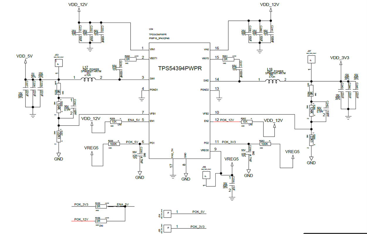
I am working with TPS54394 and we are generating two 5V outputs from 12V input. In channel 1, the output ripple seems ok, however in channel 2 the ripple of 5V output is too high.
In both channels the average output value is 5V.
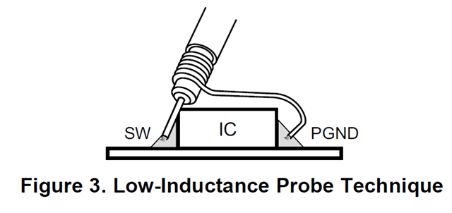
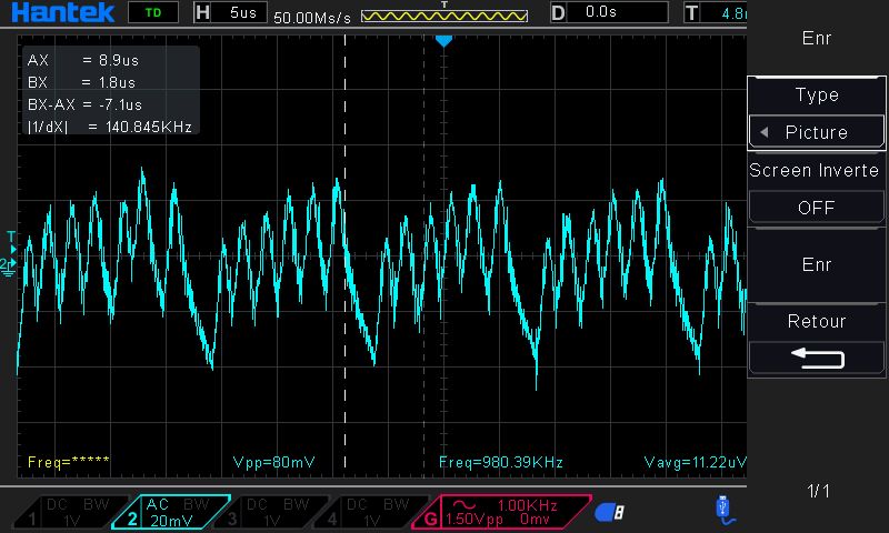
I have monitored the SW signal for both channels, in channel 1 SW seems ok, however in channel 2 is not ok, I attach image for both signals. The configuration values for capacitors, resistors and inductor is the same for both channels, as both must be 5V output.
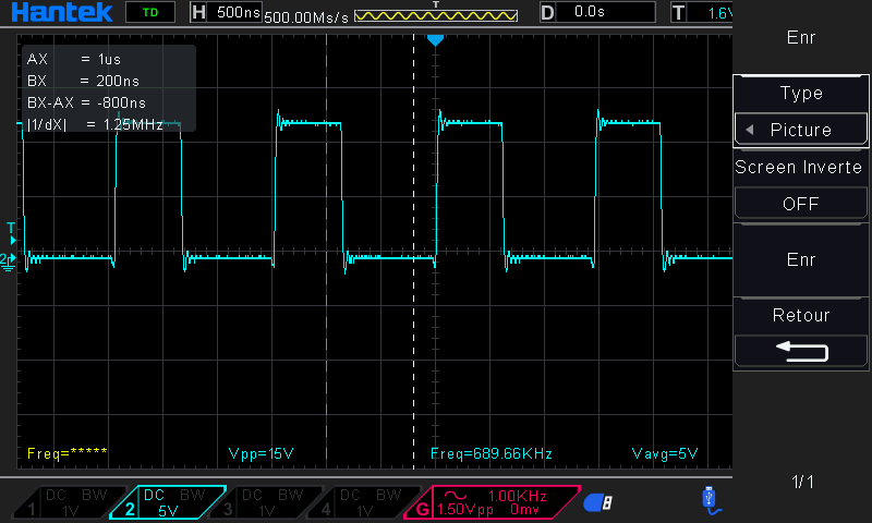
SW signal for channel 1
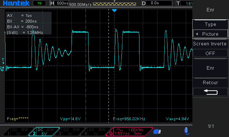
SW signal for channel 2
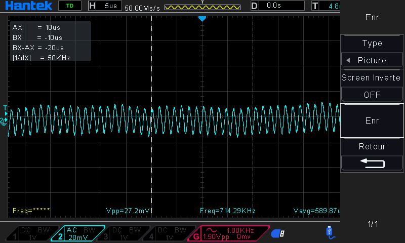
Ripple in channel 1
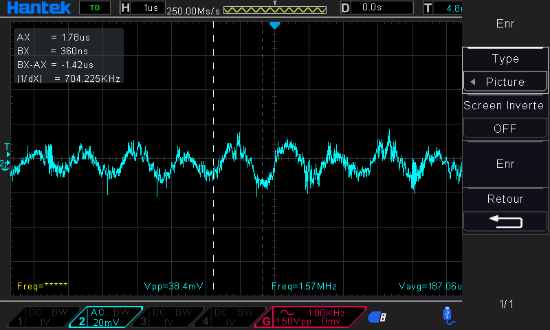
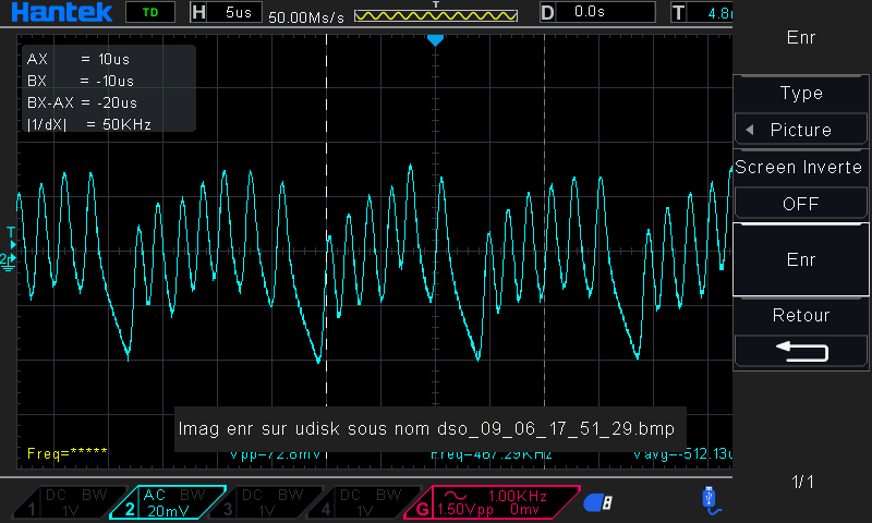
Ripple in channel 2
I would like to know what I could debug in the design to try to solve this problem, or what could be the cause related to this strage effect.
Many thanks in advance.
Kind regards
Adrián