This thread has been locked.

If you have a related question, please click the "Ask a related question" button in the top right corner. The newly created question will be automatically linked to this question.

DLP2021LEQ1EVM: I want to know the specific DMD control timing.

Part Number: DLP2021LEQ1EVM
Other Parts Discussed in Thread: DLP2021-Q1, , DLPC230-Q1

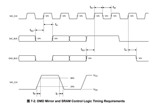
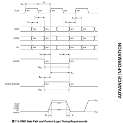
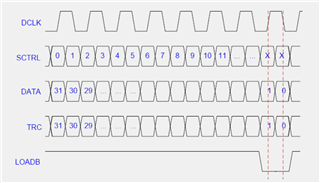
Because I want to choose my own controller to control DMD, I want to know more about the control timing of DMD.Based on the following DMD timing diagram provided by the DLP2021-Q1 document, I can't seem to figure out how to control the DMD display. I would like to know if there is a more detailed timing or content of DLP2021-Q1 control? Thank you so much for your help.

  • Hello Cherry,

    Please give our team some time to look into this issue as people are out due to a holiday.

    Do you have one of the dlp2021leq1evm? There is a user guide and control program and perhaps those could be good information and help you familiarize yourself with the design. 

    https://www.ti.com/tool/DLP2021LEQ1EVM#tech-docs

    Please also see these documentation for the dlp3021q1 which is similar and could be used as reference or for more information:

    Design Guide:

    https://www.ti.com/lit/an/dlpa086/dlpa086.pdf

    FPGA Guide:

    https://www.ti.com/lit/pdf/dlpu100

    Thanks,

    Alex Chan

  • Hello Alex Chan,

    In some special applications, when the structure and size of the product are required, we must design and develop the DMD control board ourselves. Although it is possible to buy TI's chipset and refer to the EVM schemata provided by TI, there are certainly some differences in the hardware system, and perhaps the cable connecting to the DMD is also different, so that the hardware system must be adjusted after the first design and processing. During debugging, it is found that most of the problems are between the controller and DMD, because there is no DMD interface control protocol, can not find the cause and debugging method. The above technical documentation can only help us debug the DLP2021LEQ1EVM I purchased through the GUI, and I want to debug the DMD device through my own device. Therefore, I would like to know the detailed interface control protocol of DLP2021-Q1.

    Thanks,

    Cherry 

  • Hello Cherry,

    Could you please share more details about your application?

    I want to debug the DMD device through my own device

    Are you some other device to drive /control DMD?

    regards,

    Vivek

  • Hello Cherry,

    The interface between the controller and DMD is proprietary, such that we can only provide the timing diagrams. The details of what data is sent from the controller to the DMD cannot be disclosed. The FPGA of the DLP2021-Q1 chipset should be treated as a TI ASIC, for which we only release a fully tested/validated binary firmware, just as is the case with our other DMD controllers. This is why debug is limited to ensuring the timing of the controller-to-DMD is within the datasheet specification. As you have indicated, if there is an issue between the controller-and-DMD, it is usually a result of poor signal integrity due to layout or corrupted firmware in memory. Though not the case for the DLP2021-Q1 and FPGA combination, some DMD controllers include a "training" feature in which the DMD provides feedback to the DMD to indicate the interface status/health (i.e. DLPC230-Q1).

    We will be releasing an off-the-shelf MCU controller option as an alternative to the FPGA to support the DLP2021-Q1 RTM. This MCU controller will offer a variety of host interface and memory interface options. More details will be available later this year.

  • Hello Akeem,

    Thank you for your information. In addition, I don't understand the meaning of TRC in DLP2021Q1 data manual, could you please inform me?

    Thanks,

    Cherry

  • Hi Cherry,

    TRC is toggle rate control. It's synchronous to rising edge and falling edge of DCLK. Do you have any specific question on TRC?

    Regards,

    Lori 

  • Hello Lori 

    Does this TRC mean that every time the micro mirror deflects, it will pull up once, or does it have other meanings? I don't understand what the signal level represents? Can you help me with it?

    Thanks,

    Cherry

  • Hi Cherry,

    For the DMD specification, the TRC is to reduce the data line transition frequency. TRC is provided for the data input port. Logic 1 on the TRC input commands the DMD to invert the data being clocked in to the device. Logic 0 on the TRC input specifies no data inversion.
    TRC provides clock by clock toggle rate control for DATA(9:0) and is clocked in synchronously on both the rising- and falling- edges of DCLK.

    I hope this helps.

    Regards,

    Lori 

  • Hello Lori 

    Thank you for telling me about TRC. In my understanding, the SAC_BUS logic high level is the DMD micromirror loaded down one line. The logical high level of DAD_BUS is to load a frame. Is my understanding correct?

    Thanks,

    Cherry

  • Hi Cherry,

    Please allow me look into this and get back to you soon.

    Regards,

    Lori 

  • Hi Cherry,

    The SAC and DAD buses are synchronous to rising edge of SAC_CLK, but they are a bit more complicated than you thought. The SAC and DAD buses have their own proprietary command definitions which determine the load, reset and clear states of the DMD. We have limited information that can be shared of the DMD logic specification.

    Regards,

    Lori