This thread has been locked.

If you have a related question, please click the "Ask a related question" button in the top right corner. The newly created question will be automatically linked to this question.

DLPA2005: EMI related questions : land patterns,

Part Number: DLPA2005
Other Parts Discussed in Thread: DLPC3478, DLPC3438, DLPC3470

Hi,

We have been testing the custom DLP controller board which is using DLPA2005.

During the EMI radiation pre-test in an EMI chamber, we've found that there is a problematic observed frequency at around 330 MHz which is beyond the suggested limit.

As this only happens when the projector was on, we could conclude this is related to the projector related ICs, patterns, etc: e.g. DLPC3478, DLPA2005

Although we were able to easily solve the problem by properly shielding the case, we are now optimizing the circuit design to make the EMI characteristics better.

While checking the ICs' manual, we've found some interesting parts:

The DLPA2005 datasheet link is as follows:

https://www.ti.com/lit/ds/symlink/dlpa2005.pdf?ts=1692140216596

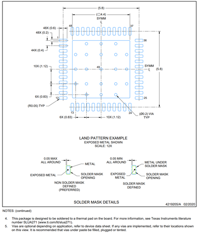
1. Via patterns (P54)

"Vias are optional depending on application, refer to device data sheet. If any vias are implemented, refer to their locations shown on this view. It is recommended that vias under paste be filled, plugged or tented."

Can I ask the reason of providing a specific grid pattern for these VIAs? I think there must be reasons, but they are not clearly stated in the datasheet.

Note that the evaluation board is also well following this guideline.

What would happen if we don't follow the guideline?

2. Layout Guidelines (P44) 

There are some guidelines on P44 and on the page, it especially emphasizes the importance of the guideline saying there would be issues in EMI if the practice is not done properly.

We wanted to narrow down the parts and during the near field probe testing, what we've found is that the radiation is more on the dmd FPCB, led cable and DLPC3478 part not from the area nearby DLPA2005.

Is this normal?

3. EMI general guidelines which is related to the custom design board which uses DLPC3478 and DLPA2005

Are there any additional materials which are related to the EMI proof design about particular parts? 

(DLPC347x, DLPA2005, etc)

Thanks.

  • Hello User,

    The team will look into your questions and get back to you.

    Best regards,

    John

  • Hi,

    thank you for your support.

    May I ask you if you have any update which is related to this issue?

    Our team has been waiting for the staff's answer, as we can apply the advice from your team.

    The question is about how to handle the EMI issue while dealing with the DLPC347x & DLPA2005 products. 

    Please drop any messages which might be useful.

    Kei Kim

  • Hello Kim,

    Thank you for your patience.

    "Vias are optional depending on application, refer to device data sheet. If any vias are implemented, refer to their locations shown on this view. It is recommended that vias under paste be filled, plugged or tented."
    What would happen if we don't follow the guideline?

    Vias under paste needs to be plugged/filled otherwise solders may get into via and cause short.

    There are some guidelines on P44 and on the page, it especially emphasizes the importance of the guideline saying there would be issues in EMI if the practice is not done properly.

    It is referring to EMI due to switching power supply.

    We wanted to narrow down the parts and during the near field probe testing, what we've found is that the radiation is more on the dmd FPCB, led cable and DLPC3478 part not from the area nearby DLPA2005.

    Is this normal?

    Your observation is correct, most common source of EMI are high frequency signals for example HS bus between controller and DMD over flex cable, input data signal via parallel port to DLPC3438.

    Typically, we have not seen LED cable causing EMI issue.

    EMI general guidelines which is related to the custom design board which uses DLPC3478 and DLPA2005

    Are there any additional materials which are related to the EMI proof design about particular parts? 

    (DLPC347x, DLPA2005, etc)

    You may want to look into other IO devices on the system.

    regards,

    Vivek

  • Thank you Vivek Thakur,

    1. Can you also check my other questions?

    - Can I ask the reason of providing a specific grid pattern for these VIAs? and What would happen if we don't follow the guideline?

    And for your answer, "You may want to look into other IO devices on the system." and my question,

    - EMI general guidelines : which is related to the custom design board which uses DLPC3478 and DLPA2005

    2. Are there any additional materials which are related to the EMI proof design about particular parts?

    As the custom board that we have developed produces shows very low EMI when the projector is off, we believe that the EMI issue is solely related to the ICs which are related to the DLP. Can you provide some materials or pages from TI or others which we can reference when implementing the custom board so that we can make a better design from EMI perspective?

    3. One more thing, in terms of the EMI concern, according to the DLPC3470's manual, the suggested bead should have the property of 600 ohm impedance at 100 MHz, but in the reference design(https://www.ti.com/tool/DLP3010EVM-LC), only 80 ohm bead(BLM15PD800SN1D) is used. Considering the fact that this bead is connected to the common ground, do you think changing it with the recommended bead with 600 ohm impedance at 100 MHz can help improve the EMI properties? (as the current EMI produces more noise at high frequency)

  • Hello Kei,

    Thank you for your questions. We are still looking into them and will get back to you by the end of the week. We appreciate your patience.

    Best,

    Maxine

  • Hi Maxine,

    Thanks. Checking up if there is any update (as it's been more than a week, I think)

    Regards,

    Kei Kim

  • Hello Kei,

    Thank you for your patience.

    Can I ask the reason of providing a specific grid pattern for these VIAs? and What would happen if we don't follow the guideline?

    There is no reason for the specific  grid pattern, you can use any pattern.  We believe the VIAS provide a good thermal connectivity to the ground plane. It helps in heat dissipation.

    Are there any additional materials which are related to the EMI proof design about particular parts?

    As the custom board that we have developed produces shows very low EMI when the projector is off, we believe that the EMI issue is solely related to the ICs which are related to the DLP. Can you provide some materials or pages from TI or others which we can reference when implementing the custom board so that we can make a better design from EMI perspective?

    We do not have any additional information or material for EMI proof design.   We do not test our EVMs for EMI.

    3. One more thing, in terms of the EMI concern, according to the DLPC3470's manual, the suggested bead should have the property of 600 ohm impedance at 100 MHz, but in the reference design(https://www.ti.com/tool/DLP3010EVM-LC), only 80 ohm bead(BLM15PD800SN1D) is used. Considering the fact that this bead is connected to the common ground, do you think changing it with the recommended bead with 600 ohm impedance at 100 MHz can help improve the EMI properties? (as the current EMI produces more noise at high frequency)

    The bead is to filter noise in the power for internal PLL clock.  Changing bead to recommended value will improve the power for PLL. I cannot comment on EMI. As mentioned earlier, we don't test the EVM for EMI.

    regards,

    Vivek