This thread has been locked.

If you have a related question, please click the "Ask a related question" button in the top right corner. The newly created question will be automatically linked to this question.

SN65DP159: HPD & I2C Connection

Part Number: SN65DP159
Other Parts Discussed in Thread: TMDS181, TPD12S016, TMDS171

Hello,

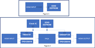
We are planning to use SN65DP159 IC to convert the TMDSTm to HDMITm and then we have connected those signals with FPGA.

For the I2C & HPD, we have used the TPD12S016RKTR level shifter.

So Can we leave HPD & I2C pins (Pin no. #4,46,47,33,39,38) of SN65DP159 IC as floating ? If no then where to connect?
We have attached the image for reference.

Thanks,

Yamini

  • Yamini

    HPD

    HPD_SRC can be left floating

    HPD_SNK must be connected to RXD_HPD (5V)

    DDC

    SCL_SRC and SDA_SRC must be connected to ground

    SCL_SNK and SDA_SNK must be connected RXD_DDCSCL and RXD_DDCSDA to configure the TMDS_CLOCK_RATIO_STATUS bit.

    Are you using the DP159 as a retimer between a DC-coupled HDMI to a AC-coupled FPGA?

    Thanks
    David

  • Hi David,

    Thanks for the quick response.

    We have updated our connections as per your suggestion. Please find attached our schematic. it would be great if you can review and let us know your comments.

    We are using the DP159 as a retimer between a DC-coupled HDMI input to an AC-coupled FPGA and an AC-coupled FPGA to a DC-coupled HDMI output. Also, find the top-level block diagram for your reference.

    53-21001-00-00_HDMI_IN_OUT.pdf

    Thanks,

    Yamini

  • Hi Yamini

    Please see attached for my schematic review comments.

    53-21001-00-00_HDMI_IN_OUT_TI_Reviewed_06012021.pdf

    But if it is a DC-coupled HDMI input, you need to use the TMDS181. 

    Please also work with the PI team to have them reviewed the TPD12S016.

    Thanks

    David

  • Hi David,

    Thanks for the schematic review.

    So You means to say to use TMDS181 IC  instead of SN65DP159 on the HDMI Input side , Correct?

    Thanks,

    Yamini

  • Hi, Yamini

    Correct, for DC-coupled HDMI input, you want to use TMDS181. 

    The DP159 is for AC-coupled HDMI input, or DP++.

    Please double check and make sure the input is DC-coupled as your schematic says the input is AC-coupled.

    Thanks

    David

  • Hi David,

    Our input to FPGA is generic HDMI. It may be either from laptop, desktop, tablet, android phone etc. So which IC will be more suitable in our product on the HDMI input?  FYI... our input to FPGA works on FHD at 60Hz.

    And output from FPGA works on FHD at 120Hz and our HDMI output will be connected to any screen which supports 120Hz So can SN65DP159 IC supports FHD at 120Hz on the output side?

    Thanks,

    Yamini

  • Yamini

    Our input to FPGA is generic HDMI. It may be either from laptop, desktop, tablet, android phone etc. So which IC will be more suitable in our product on the HDMI input?  FYI... our input to FPGA works on FHD at 60Hz.

    Most generic HDMI is DC-coupled HDMI, so you should use the TMDS181.

    And output from FPGA works on FHD at 120Hz and our HDMI output will be connected to any screen which supports 120Hz So can SN65DP159 IC supports FHD at 120Hz on the output side?

    FHD at 120Hz is 3G per lane, DP159 can support it.

    Thanks

    David

  • Hi David,

    Thank you for quick response. We have updated our schematic to include TMDS181 on input side. Can you please verify the attached schematic and let us know if any changes are required or not? Also can you let us know the availability and End of life status for TMDS181 and SN65DP159.

    ThanksHDMI_IN_OUT_04June2021.pdf
  • Hi,

    Do you have common mode choke on the DP159 output? I would add the choke for EMI purpose and also addressing the HDMI inter-pair skew requirement. Otherwise the schematic looks ok.

    We do not plan to EOL the TMDS181 or the DP159.

    Please check with your TI local office for TMDS181 and DP159 availability.

    Thanks

    David

  • Hi,

    Can you share reference for the what you are trying to say like any schematic which we can refer for it.

    Thanks,

    Yamini

  • Hi, Yamini

    Please see DP159 schematic for the choke reference.

    Thanks

    David

  • Hi David,

    TMDS181 IC  is not available at present and also it has the longer Lead-times So can you suggest any alternate IC?

    Thanks,

    Yamini

  • Hi, Yamini

    Do you need HDMI1.4 (3G) or HDMI2.0 (6G)? If only HDMI1.4, then you may take a look at the TMDS171. Otherwise the TMDS181 is the only HDMI2.0 DC-coupled HDMI retimer we have.

    Thanks

    David

  • Hi David,

    TMDS181 IC supports on lower than HDMI 2.0 as a retimer mode?

    And TMDS181 IC & TMDS171 both are pin to pin compatible?

    For now, We will use TMDS171 and later on can it replace with TMDS181 (When available) without changing any components?

    Thanks,

    Yamini

  • Yamini

    The TMDS181 and TMDS171 are pin-to-pin compatible with each other. 

    TMDS181 retimer by default is automatically activated at pixel clock approximately above 100 MHz when jitter cleaning is needed for robust operation when this option is enabled (default). The retimer operates at about 1 Gbps to 6 Gbps data rate. But you can change the TMDS181 redriver/retimer configuration through register 0x0A, DEV_FUNC_MODE bits.

    Thanks

    David

  • Hi David,

    Thank you for the response.

    We have questions regarding the EDID.

    1) Do we need the EDID EEPROM ?

    If yes, then where we connect because we have refer some of the reference schematic.

    And In the ref schematic , EEPROM is directly connected with DDC line of the HDMI Input(RX side) .See Figure 1 in the below image.

    And other ref schematic, EEPROM is connected with DDC line (SCL_CTL,SDA_CTL) of the Input (TMDS181 ) and output (SN65DP159) ICs and that connection are also connected with FPGA & Clock IC. See Figure 2 in the below image.

     2) Also, How EDID is managed in both TMDS ICs?

    Thanks,

    Yamini

  • Yamini

    Per the HDMI spec, all sink shall contain a CEA-861-D compliant E-EDID data structure accessible through the DDC bus.

    For your design, is the FGPA acts as a sink, a source, both, or just pass through the HDMI traffic?

    Thanks

    David

  • Hi David,
    In our case, FPGA acts as a both. In our design FPGA takes the signal from HDMI Input, processes it, and then it passes the signal to the HDMI Output. So for HDMI input, it acts as a sink and for HDMI out it acts as a source.


    We have one more query. TMDS181 and SN65DP159 both ICS support HDMI 2.0 so can we use HDMI 2.1 or we can use only till HDMI 2.0?
    Thanks,
    Yamini

  • Yamini

    In this case, the FGPA Sink side should have a EDID. The FPGA source side should read the EDID information from the monitor.

    Both the TMDS181 and DP159 only support HDMI2.0, they do not support HDMI2.1.

    Thanks

    David

  • Hi David,

    Thank you for your support.

    We have some question regarding the SN65DP159 , TMDS181 ICs.

    1) We are using TMDS IC on the Input side and SN65 IC on the output side. Our input to FPGA is generic HDMI. It may be either from laptop, desktop, tablet, android phone etc. and our HDMI output will be connected to any screen. But by mistake if we swap the connection like HDMI input cable will be connected with screen and output cable will be connected with laptop then what happed with the both IC? How we can know that the connection are wrong using the IC.

    2) We are using CAPs on the output signal of the TMDS IC and input signal of SN65 to convert DC to AC coupled or AC to DC coupled so is there any losses in the signal?

    3) Can you please verify the attached schematic specifically the I2C , HPD connection for the both IC.

    let us know if any changes are required or not?

    Thanks,

    Yamini

    4760.HDMI_IN_OUT.pdf

  • Yamini

    1. On the TMDS181 side, the sink is expecting to see 5V. But since there is no 5V present, the sink will not enable its HPD to indicate the presence of the sink.

    On the DP159 side, the source will drive 5V and you will also drive 5V, and this will cause 5V power contention and may cause damage to your power circuit.

    2. On the TMDS output, since you are using external 50ohm termination to 3.3V, this will create a double termination and cut the output signal amplitude in half. You have to use the TMDS181 VSADJ to compensate for the drop in signal amplitude. The DP159 is ok.

    3. I looked at the HPD and DDC implementation and they looked ok. Since the FPGA is in the middle, the FPGA needs to handle the HPD and DDC communication between the input and the output.

    Thanks

    David