This thread has been locked.

If you have a related question, please click the "Ask a related question" button in the top right corner. The newly created question will be automatically linked to this question.

DS110DF410: About the DS110DF410 debugging process encountered some problems

Part Number: DS110DF410

Dear Expert

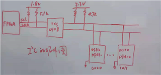
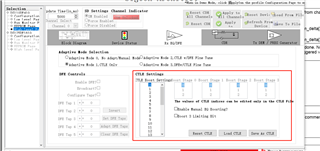
1. What is the meaning of RWSC as shown in the figure below?Is setting this bit, 0x2F[0] to 1, going into CTLE's adaptive mode?In this mode, instead of setting the EQ seting value, the device will automatically find the most appropriate value?

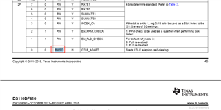
2. As shown in the figure below, when I select Adaptive Mode 1, does the CTLE Setting have to be set manually?If so, how?

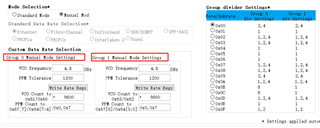
3. As shown in the figure below, what are the differences and meanings between Group 0 and Group 1?The specifications don't seem to describe it.

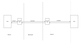
4. The following diagram is the topology of the link using DS110DF410 on our product.As you can see, we've added DS110DF410 at both the transmitter and the receiver.The routing length of each link segment is shown in the figure.Currently we are commissioning at a rate of 4.8Gbps (it is possible to increase to 9.6Gbps later)

It is hoped that the engineer of the original factory can configure a set of register tables according to the rate of 4.8Gbps and the actual wire length below (PCB plate is TU768+TU872).The Adaptive Mode 1 is sufficient.

  • Hello Gabriel,

    1. RWSC stands for read write self-clearing. In other words register 0x2F[0] can be written to, read from, and is self-clearing every time it is set high. Setting register 0x2F[0] = 1 will initiate adaptation of the CTLE. When register 0x2F[0] is set high the DS110DF410 attempts to find a set of CTLE setting that produces a better adaptation figure of merit than the starting CTLE values.

    2. No, the CTLE does not have to be set manually.

    3. There are two VCO running frequency groups for the retimer that are referred to as “Group 0”, for 1 GbE, and “Group 1”, for 10 GbE.

    4. Section 3.10 Manual Data Rate Configuration in the following programmer's guide will explain how to program the device for a 4.8GBps data rate.  www.ti.com/.../snla323.pdf

    Regards,

    Kia Rahbar

  • Hi Kia

    (1) The topology of the IIC interface of DS110DF410 connected with FPGA is shown below

    (2) The timing diagram of SDA and SDC signals output from FPGA is shown below, in which the SCL frequency is about 150kHz

    (3) The problem encountered is: the IIC interface of DS110DF410 has no answer;Would like to consult what may be the reason.The power supply has been tested and there is no problem.

  • Hello Gabriel,

    Can you please probe the output of the TXS0108 to ensure the data has been transmitted through this device properly? I believe the issue might be due to the way the TXS0108 is configured. For further help on TXS0108 configuration, please make a post on the logic forum.

    Regards,

    Kia Rahbar