This thread has been locked.

If you have a related question, please click the "Ask a related question" button in the top right corner. The newly created question will be automatically linked to this question.

SN65DPHY440SS: Re-Timer Unexpected Drive Change

Part Number: SN65DPHY440SS
Other Parts Discussed in Thread: DPHY440SSRHREVM

Hello,

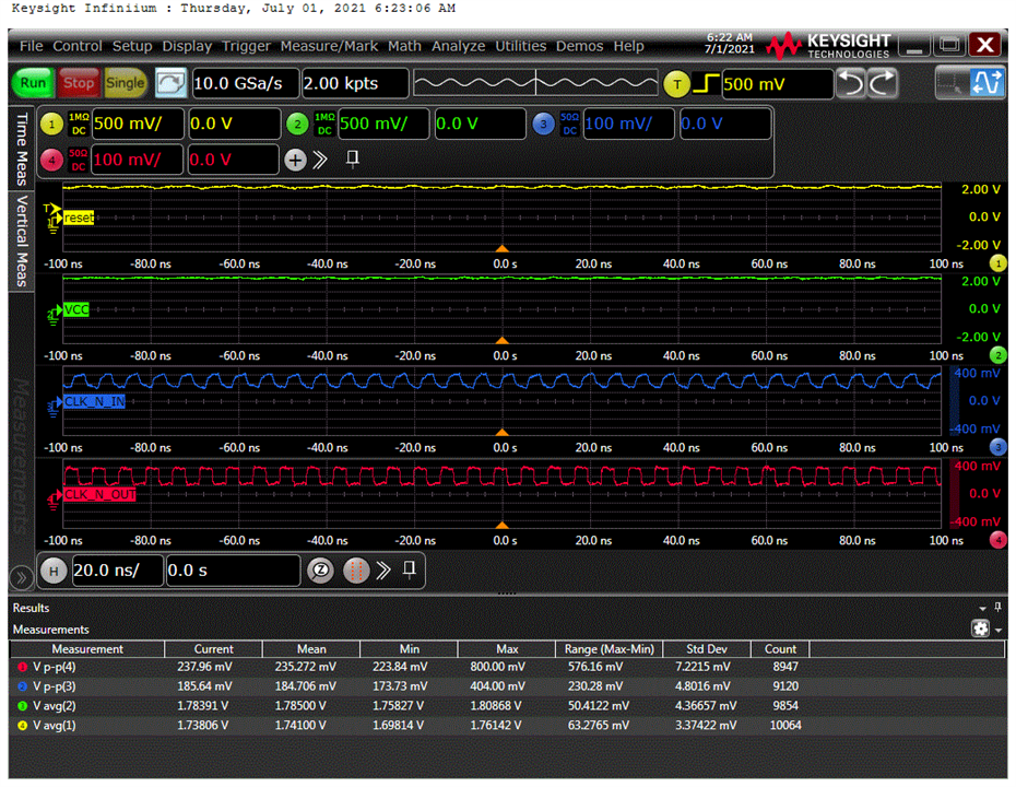
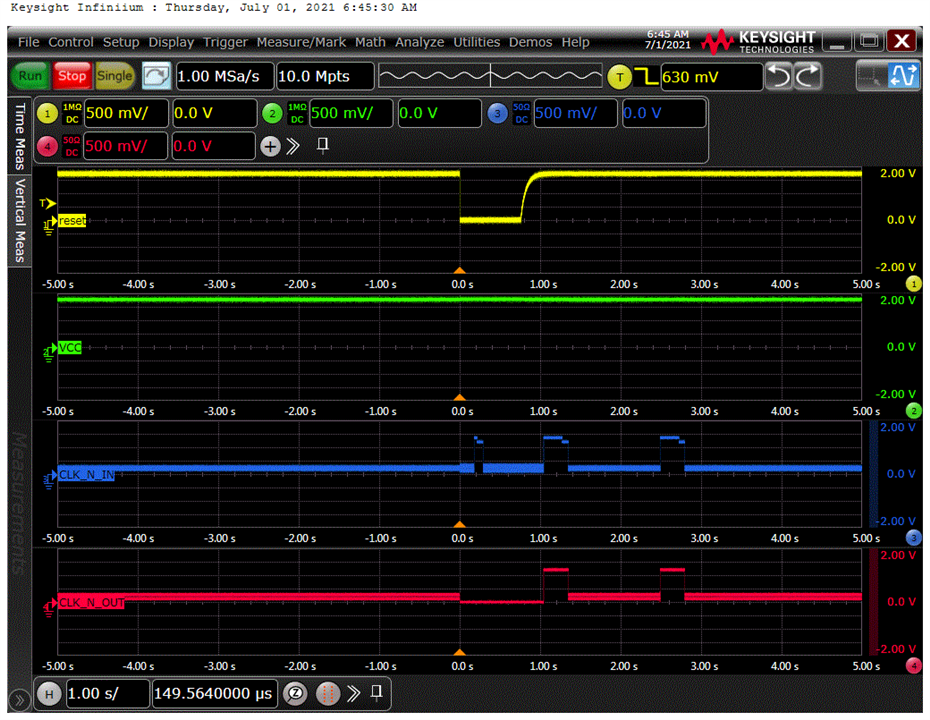
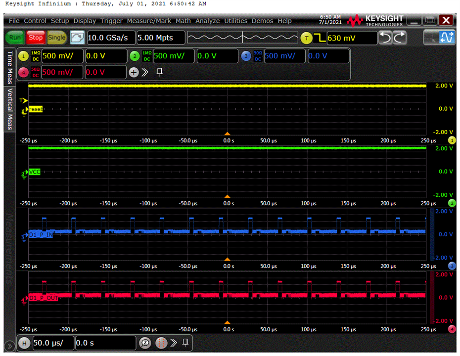
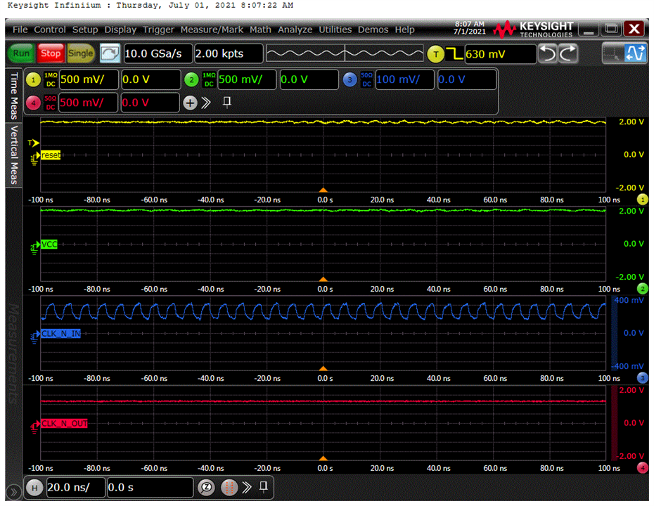
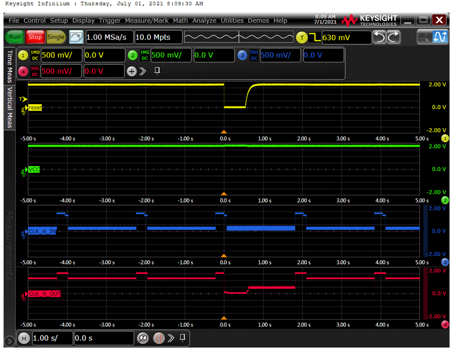
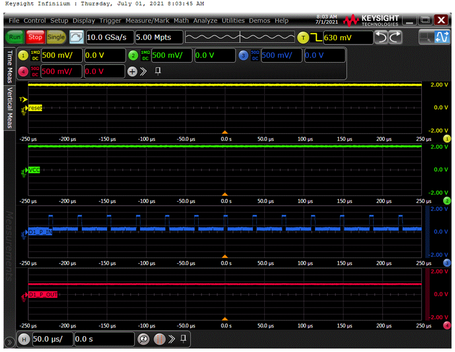
I'm running into a problem with this part. First, a little back story. I've already verified the part works in my system using the eval board. Now I've brought the Re-Timer IC onto my own PCB with the same configuration and it doesn't work anymore. I've verified Data and Clock are passing through the Re-Timer and appear to be output as expect. However, one interesting thing I've noticed is that the output driver appears to unexpectedly (and periodically) change its driving condition. Please see attached scope capture.  
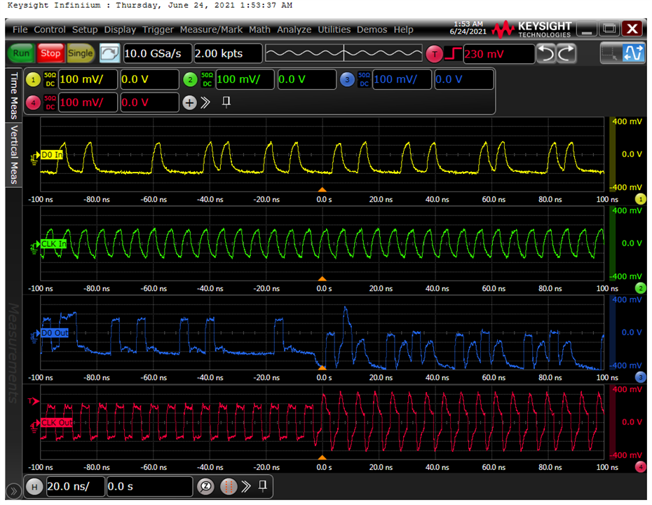
As you can see the input data and clock signals do not change yet the output goes through a drive change.

Any help is appreciated.

Thank you,

Nathan

  • Nathan

    Is this a MIPI-CSI or a MIPI-DSI design? 

    For the MIPI-CSI application, instead using D0, can you switch to D1, D2, or D3?

    Does the clock go through LP/HS or always stay in the HS state?

    Thanks

    David  

  • MIPI-CSI. 

    Sorry for the confusion on data labelling. D0 is the label for my circuit, however it's passing through D3 on the re-timer. The clock is always in HS state but the data goes between HS and LP.

    For a little more info I'm using 2 data lanes, which pass through D2 and D3 of the Re-Timer. The other data inputs are grounded with their outputs left open.

    Thanks,

    Nathan

  • Nathan

    Are you using I2C to control the DPHY440?

    With the clock always in HS state, can you write to the DPHY440 registers to always enable clock in the high speed state?

    (Address, Data)

    (0x50, 0x10), // HS TX path Override enable
    (0x51, 0x10), // HS TS path enable
    (0x61, 0x0F), // Disable LP path.
    (0x70, 0x10), // HS RS path Override enable
    (0x71, 0x10) // HS RX path enable​

    Thanks

    David

  • I am not using I2C but I get it setup to make those changes. In the mean time, do you know if the evaluation board (DPHY440SSRHREVM) is configured to always enable clock in the high speed state? This same system worked with the eval board.

    Thanks,

    Nathan

  • Nathan

    I made one mistake in my previous response

    (Address, Data)

    (0x50, 0x10), // HS TX path Override enable
    (0x51, 0x10), // HS TS path enable
    (0x61, 0x00), // Disable LP path.
    (0x70, 0x10), // HS RS path Override enable
    (0x71, 0x10) // HS RX path enable​

    DPHY440 comes up in its default state unless configured through its I2C register, so my expectation is that the DPHY440 on the EVM is in the same state as the DPHY440 on your board. 

    Any chance you can put the DPHY440 EVM back in your setup and verify the EVM still works?

    Can you also check and see the device connected to the DPHY440 output is not trying to go into the LP state?

    Thanks

    David

  • David, 

    I've changed the registers as you've suggested and I'm no longer getting an output. I've also tried resetting the re-timer and it still does not output anything. I have verified the DVM still works though. I'm fairly positive the device connected to the re-timer output is not trying to go into the LP state because the clock always stays in HS with the DVM connected. However, I'm not able to check the firmware to confirm at this time.

    Thanks,

    Nathan

  • Nathan

    Can I take a look at your schematic? Can you also check the DPHY440 power up sequence and see if the power sequence is the same between your design and the EVM? 

    Thanks

    David

  • David,

    Just to clarify, would checking the power sequence mean probing VDD, VCC, and reset on power on? Also, could I get your email for sending the schematic?

    Thanks,

    Nathan

  • Nathan

    Would you please accept my friendship request and then you can send me the schematic in a private message?

    Besides VCC, VDD, and Reset, I will also check both the clock and data lane to make sure both of them are driving LP11 until the DPHY440 comes out of the reset.

    Thanks

    David

  • Hi David,

    Here are a couple scope captures coming out of reset. 

    Here is a capture with Reset, D0_N (Single Ended), VCC, and CLK_P (Single Ended)

    And a capture with Reset, D0_N (Single Ended), VDD and CLK_P (Single Ended)

    It looks to me like the DPHY440 is not putting the clock and data lines into LP11 during reset. Does this give you any better insight into what's going on?

    Thanks,

    Nathan

  • Nathan

    Is D0_N and CLK_P the DPHY440 output? Can you please capture the input waveform and comparing against the EVM?

    Thanks

    David 

  • David,

    I've captured the waveforms for the EVM and will post them now and then re-run the same set of captures with the re-timer on my PCB in another reply. I only have a 4 channel scope so I probed VCC for these captures and then probed VDD after to verify its functionality.

    Again, this is only using the EVM:

    VCC does not change from 1.8V regardless of Reset State.

    VDD is nominally 1.2V and goes to 0V upon Reset low. It returns to 1.2V before Reset has finished charging back to high.

    Here are a couple captures of Reset, VCC, CLK_N (before re-timer), and CLK_N (after re-timer)

    Nominal:

    On Reset:

    Here are a couple captures of Reset, VCC, DA2_P, and DB2_P (after re-timer)

    Nominal:

    On Reset:

    It looks to me like my system is set up to run a continuous clock and data switches between LP and HS. On Reset low, the outputs of the Re-Timer go to zero. When reset returns high we can see both clock and data exhibit a couple of extended LP states before settling into their nominal conditions.

    Thanks,

    Nathan

  • Here are the same captures using the re-timer on my PCB:

    VCC does not change from 1.8V regardless of Reset State.

    VDD is nominally 1.8V and goes to 0V upon Reset low. This appears to exhibit a noticeably different behavior to the EVM so I took a scope capture that I'll place here:

     The rest of this reply will mimic the above reply for ease of comparison.

    Here are a couple captures of Reset, VCC, CLK_N (before re-timer), and CLK_N (after re-timer)

    Nominal:

    On Reset:

    Here are a couple captures of Reset, VCC, DA2_P, and DB2_P (after re-timer)

    Nominal:

    On Reset:

    I'm still stumped but I think we're getting somewhere. 

    Thanks again,

    Nathan

  • Nathan

    Your clock and data have a DC offset. I can't tell if it comes from the measurement setup or the board. Can you double check and verify you have a solid connection between the DPHY440 thermal pad and the board ground? We recommend at least 75% solder coverage between the thermal pad and the board ground.

    Thanks

    David 

  • David,

    Thanks for the response. I do have a large thermal pad with multiple vias tied directly to the ground plane. There is sufficient solder making that connection as well.

    I'm not sure if this could be due to noise but the PCB does have an input and output ground plane in which the differential signals cross over both. I did this to avoid ground loops when connected to the evaluation board. To remove any doubt I have laid out a new PCB that should minimize any noise and grounding problem. I will update once the new PCBA is tested.

    Thanks,

    Nathan

  • Nathan

    Sounds good, please keep me updated once you received your new PCB.

    Thanks

    David 

  • Hi David,

    The new PCB has been assembled and I'm now confident the issue is not related to noise. I'm back to square one where the outputs looks like the original scope capture in this thread with the strange drive change. I have not changed the registers on this new pcb since that appeared to give the outputs the DC offset.

    I'm considering doing a register comparison between the re-timer on the EVM and my PCB. Do you think this would be a worthwhile effort? Do you have any other suggestions?

    Thank you,

    Nathan

  • Nathan

    Default register value is the same between the EVM and the PCB, so I am not sure how much that will help.

    Any chance you can share the layout file in the private message? I am curious on how the ground is being handled in the design. Also when you are probing the signal, which ground are you using as your probe ground reference?

    The amplitude of the signal in the scope waveform looks to be doubled, which seems to me that the DPHY440 is disabling its high speed termination. The DPHY440 only disables its high speed termination when going into the LP mode, but I am not seeing the 1.2V amplitude for the LP mode in the scope plot.

    I assume the EVM still works with the new PCB?

    Thanks

    David