This thread has been locked.

If you have a related question, please click the "Ask a related question" button in the top right corner. The newly created question will be automatically linked to this question.

SN65DP159: abnormal clock output after several times hot-swap

Part Number: SN65DP159

Hi, expert

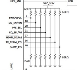
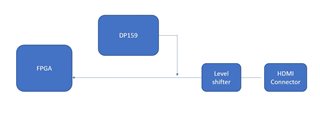
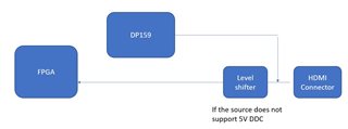
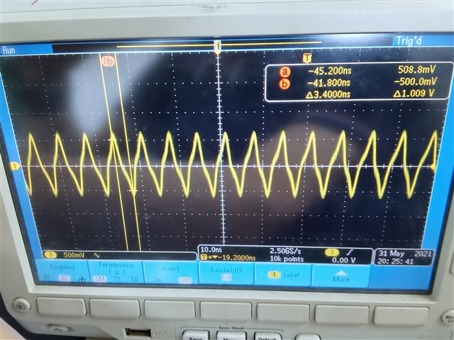
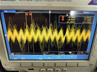
My customer met an issue on SN65DP159 --- the clock outputs are abnormal, please see attached waveforms and their schematic.

This issue happened with HDMI2.0 and HDMI1.4, and HPD_SNK is high when the issue happened. 

Could you please help review the schematic and find out if there are any design errors especially the pull up and pull down pins?

And could you please tell customer which pairs of I2C should be used to debug? Thanks.

HDMI_2.0.pdf

Best Regards.

Chen

  • Chen

    Looking at the schematic

    1. Do you have external pulldown capacitor on the OE pin? Please make sure you are meeting the DP159 power up requirement as listed in its datasheet.

    2. Recommend to have common mode choke on the output for EMI purpose

    Can you please dump out the DP159 Page 0 and Page 1 registers between the good output case and the bad output case? Page 0 registers are in the DP159 datasheet. For Page 1 registers, please write 0x01 to register 0xFF, and then dump from 0x00 to 0xB1.

    Can you also swap the DP159 between the two boards to see if the issue follows the unit or the board?

    Thanks

    David

  • Hi, David

    Thanks for your reply. Customer still have several questions to confirm, could you please help on it?

    1. Which pair of I2C interfaces should them use to write registers.

    2. They have not added pull down capacitor at OE pin. Which function will this capacitor matter?

    3. What are distinction among the functions about SRC, SNK and CTL I2C interfaces?  


    Best Regards.

    Chen

  • Chen

    1. Which pair of I2C interfaces should them use to write registers.

    *** SCL_CTL and SDA_CTL (pin 15 and 16)

    2. They have not added pull down capacitor at OE pin. Which function will this capacitor matter?

    *** Please refer to section 9.3.1 and 9.3.2, you need the capacitor on the OE pin to ensure proper power-up timing

    3. What are distinction among the functions about SRC, SNK and CTL I2C interfaces?  

    *** SCL_CTL and SDA_CTL -> Programming DP159 registers

    *** SCL_SRC and SDA_SRC, part of the DDC bus used to communicate EDID between the source and the sink. Connect to the source side as needed

    *** SCL_SNK and SDA_SNK, part of the DDC bus used to communicate EDID between the source and the sink. Must be connect to the sink side

    Thanks

    David 

  • Hi David 

    Thanks for your reply! There are three further questions need your kindly help.

    1. Besides the OE and common mode choke problems, what else design flaws may exists in customer's design?

    2. There are some pull up and pull down resistors remaining in the schematic of datasheet, but customer has not leave the room for these resistors in their design, does it matter?

    3. As you recommended, connecting SRC I2C to ground and connecting SNK I2C to FPGA, are there any problems as the pull up voltage of SNK is 5V while the pull up voltage of SRC is 3.3V? Will external interference applied to FPGA through SNK I2C?


    Best Regards.

    Chen

  • Chen

    1. I don't see any other issue with the schematic, but we should also review their layout if possible.

    2. I2C_EN must be pulled high or low to select between pin-strap and I2C mode. HDMI_SEL must be pulled high or low to select between DVI and HDMI. Everything else can left floating base on their design.

    3. If FPGA requires 3.3V DDC, then they will need an external level shifter to shift from 5V DDC to 3.3V DDC.

    Thanks

    David

  • Hi, David

    Please see attached PCB files.

    As for suggestion #3, can I take it as connecting SRC I2C to ground, and connecting SNK I2C from HDMI port to SN65DP159 then connect to FPGA through a level shifter?

    HDMI.PcbDoc

    Best Regards.

    Chen

  • Chen

    As for suggestion #3, can I take it as connecting SRC I2C to ground, and connecting SNK I2C from HDMI port to SN65DP159 then connect to FPGA through a level shifter?

    Please see below block diagram for the DDC snooping implementation

    Looking at the layout, 

    1. It looks like the clock is coming from J14 connector while the data is coming from J15 connector, is the clock and data come from the same source?

    2. Layer 4 is labeled as VCC, is is a power plane?

    3. Recommend they create power plane for the 1.1V and 3.3V instead routing them as traces

    4. Recommend they place the power decoupling caps on the bottom layer and connect the caps between the 1.1V/3.3V power plane and the DP159 thermal pad. 

    When the issue happens, can they also measure the clock input as well?

    Thanks

    David 

  • Hi, David,

    Please see below reply,

             1、The clock and data are came from the same FPGA source.

             2、LAYER 4 is a power layer.

             3、1.1V and 3.3V are divided from the power layer.

             4、Do you mean put all the decoupling caps on the bottom layer and connect the ground to PAD?

             5、The input clock is normal when the issue happend.

    Best Regards.

    Chen

  • Chen

    I made one mistake in my previous block diagram, please see the updated block diagram.

    With the HDMI trace being routed on layer 3 and layer 4 is the power layer, are there sufficient distance between Layer 3 and 4 to minimize the power crosstalk between them?

    They should put the power decoupling caps on the bottom layer, and have them via directly to the DP159 thermal pad and the 1.1V/3.3V power plane.

    Have they done the unit swapping test yet?

    Thanks

    David