This thread has been locked.

If you have a related question, please click the "Ask a related question" button in the top right corner. The newly created question will be automatically linked to this question.

DP83869HM: rbias sgmii fcs errors, not stable connection

Part Number: DP83869HM

Hello,

I want share my experience with  DP83869HM.

I have 2 custom boards. One working Ok, other sgmii connection very unstable.
Linux  ethtool -S eth0  show fcs errors.
After investigation, I  found cause of not stable sgmii connection via sgmii.
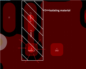
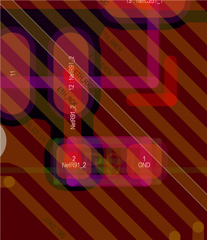
Cause was very small parasitic capacitance between RBIAS copper solder plane ant RGMII data lines planes at second layer. See picture:

To solve this problem need  DE soldering chip and rbias resistor, isolate chip rbias contact, connect rbias copper plane to gnd(use as shield), and solder rbias 11k resistor  directly to chip rbias contact and GND. 
This tested and working Ok, but some difficult. 

Possible light solution. Connect in parallels rbias resistor, 33pF  capacitor. But not all noise avoid.
What can I use biggest capacitance?  Is ok 0.1uF capacitor ?


I not found in application notes warnings about rbias sensitivity.  Only - "rbias" must be close to chip. 


Other problem I see with  DP83869HM. This chip don't  have ground pins, only pad. Pad must be connected to GND using via. So power coupling capacitors current  must use  vias.
Via have big impedance at high frequency. 

What  minimum via count and size must have pad connection with GND?

It seems to me that:

1.  Rbias must have dedicated via to pad (avoid noise).  Its true? Why rbias not included into chip? 

2. Is  quartz  generator capacitors ground must have dedicated via to pad?

3.  Which not used pins possible connect to pad ant GND?  For better decoupling. To avoid vias   (examp.: JTAG)

B.R.

Darius Babrauskas


  • Hi Darius,

    We are looking into your questions and will be able to provide additional feedback by Wednesday of this week.

    Thank you,

    Nikhil

    All information in this correspondence and in any related correspondence is provided “as is” and “with all faults”, and it is subject to TI’s Important Notice (http://www.ti.com/corp/docs/legal/important-notice.shtml).

  • Hi Darius,

    To answer some of your questions:

    • We have seen some distortion improvements with a parallel cap to RBIAS from 33pF to 250 pF. We have not tested anything larger. 
    • The 1% tolerance for RBIAS is more easily included in the design as an external component. 
    • Decoupling caps should be placed close to the pins of the PHY as instructed by the datasheet. If the PHY is on the top of the board, we often place the decoupling caps on the bottom of the board, so the GND pin of the caps have a clean path to the GND pad of the PHY. 

    Has the root cause of the issue truly been identified as the unstable RBIAS signal? You may refer to this troubleshooting guide, with a section on forming an SGMII link for more info: https://www.ti.com/lit/an/snla246a/snla246a.pdf?ts=1632421799498&ref_url=https%253A%252F%252Fwww.google.com%252F

    Thank you,

    Nikhil

    All information in this correspondence and in any related correspondence is provided “as is” and “with all faults”, and it is subject to TI’s Important Notice (http://www.ti.com/corp/docs/legal/important-notice.shtml).


  • >>Has the root cause of the issue truly been identified as the unstable RBIAS signal?

    Yes its truly. I am sure 99,99% Slight smile.  Our old custom board (version 1) don't have this issue, because rbias plane was shielded  with internal GND planes (not special). 
    It seem to me, that this issue need insert into  troubleshooting guide. I lost 2 weeks to solve this problem. RBIAS copper plane must be GND shielded from second layer. 

    We try with a parallel cap to RBIAS 33pF,  220 pF.  But these tests did not help us. We got  fcs errors, when do ping test with 10000 bytes packets from 2 terminals windows.

    Have you recommendations, how many via need  to connect  pad with GND plane on second layout layer?

    Thank you,

    Darius

  • Hi Darius,

    Can you elaborate on what is meant by "RBIAS plane was shielded with internal GND planes"? We do not have any special via configuration for connecting RBIAS to the GND plane and have not seen this issue before. The screenshot you have shown looks ok.

    Are you checking for errors on the MAC side or the PC side?

    Thank you,

    Nikhil

    All information in this correspondence and in any related correspondence is provided “as is” and “with all faults”, and it is subject to TI’s Important Notice (http://www.ti.com/corp/docs/legal/important-notice.shtml).

  • Hi Nikhil,
    >>Can you elaborate on what is meant by "RBIAS plane was shielded with internal GND planes"? 

    Our boards is multilayer ( 8layers).  So in old board version 1  between RBIAS copper plane and eth data signal layer exist GND plane(polygon). So this board don't have issue.  Board version 2   eth data signal layer are on second layer. This board have issue. Layer thickness 0.125mm.  Rgmii signals are 3.3V  ~25Mhz (fast rising, fall signals ).   We have her small parasitic  capacitance (maybe 1pF)  between  RBIAS copper plane and eth signals.  So we have capacitance divider - parasitic capacitance and rbias input capacitance(maybe 10pF).  In result we got noise on rbias input.  Only "GND shield" between rbias and eth signals can help.  Additional capacitance 33pF or 220pF in parallel to RBIAS not help. 

    >>Are you checking for errors on the MAC side or the PC side? 

    We using DP83869HM  as bridge, sgmii on PC (embedded linux with sgmii interface) side, rgmii mac on  micro controller side. So I checking FCS errors on PC side, with command "ethtool -S eth0" on terminal console  and doing "pings" from 2 terminal consoles (PC side).  So I have 3 test consoles.  This setup simplified my test.

    I try find and read "errors registers" on DP83869HM. But they not show any errors. 
    Image1. show linux console fcs errors if use board version 2. Fcs errors not show on old board version 1.


     >>We do not have any special via configuration for connecting RBIAS to the GND plane and have not seen this issue before. The screenshot you have shown looks ok.
    Because rbias is very sensitive part, it seem to me, that rbias resistor gnd must be connected to  DP83869HM  GND PAD with dedicated track (signal GND). I see, that this point can be make ease,  with  thin track on same layer through the corner of chip. This avoid gnd common mode noise (CMN). And rbias signal pad must be "gnd shielded"  from other signals.   "gnd shield"   must be connected at 1 point  through  via to DP83869HM  PAD (avoid CMN noise on shield).


    B.R.

    Darius

  • Hi Darius,

    We are looking into your questions and will have additional feedback by early next week.

    Thank you,

    Nikhil

    All information in this correspondence and in any related correspondence is provided “as is” and “with all faults”, and it is subject to TI’s Important Notice (http://www.ti.com/corp/docs/legal/important-notice.shtml).

  • Hello Darius, 

    I am covering for nikhil,

    Do you have any question or need any additional support here?

    Please note that a 15 pF or 22 pF parallel cap is recommended.

    Regards,

    Sreenivasa

  • Hello Sreenivasa,

    Currently we use:

    1. "To solve this problem need  desolder chip and rbias resistor, isolate chip rbias contact, connect rbias copper plane to gnd(use as shield), and solder rbias 11k resistor  directly to chip rbias contact and GND. "

    >>Please note that a 15 pF or 22 pF parallel cap is recommended.

    The parallel cap don't help to resolve for our problem. I don't try this cap on modified board, because it working nice. But in future I will try. 

    Thank you. 

    B.R.

    Darius

  • Hello Darius

    Thank you for the detailed inputs.

    For my understanding, Did you have a separate polygon for Rbia  or did you route the Rbias ground ? Was the next layer a routing layer - was this a 4 layer board ?

    Regards,

    Sreenivasa

  • Hello Darius

    Could you please answer the below.

    For my understanding, Did you have a separate polygon for Rbias  or did you route the Rbias ground ? Was the next layer a routing layer - was this a 4 layer board ?

    Regards,

    Sreenivasa

  • Hi Sreenivasa,

    Our board is 8 layer.

    In picture you can see 2 layers (component  and  second (next) internal layer). I disabled others layer for better view.
    After our modification (isolating 12 chip contct) NetR91_2 polygon became isolated and we it routed to GND poly. (It became shield) .
    Rbias resistor R91 we solder on air between  12 chip contact and GND.

    B.R.
    Darius


  • Hello Darius

    Thank you for the explanation and appreciate.

    NetR91_2 polygon became isolated and we it routed to GND poly. (It became shield) .

    Could you please elaborate a bit.

    Regards,

    Sreenivasa


  •  I append picture with only component layer.

    To avoid parasitic capacitance between  rbias and rgmii  signals,  need insert gnd plane between ( NetR91_2 )

  • Hello Darius

    Thank you and understand. Pin 12 is now floating and you are connecting to the resistor externally.

    Please let me know if you have any other questions or inputs. If not it would help if could close the thread as resolved.

    Regards,

    Sreenivasa

  • Hello Darius

    If you do not have any additional inputs, please close the thread by clicking the resolved button.

    Regards,

    Sreenivasa