Part Number: DP83867IS
Hi all
Would you mind if we ask DP83867IS?
This question is relation to following forum;
https://e2e.ti.com/support/interface-group/interface/f/interface-forum/1042203/dp83867ir-during-latch-in-of-hardware-configuration-pins
Our customer uses DP83867IS with SGMII. PHY address setting conditions are follows;
-0x0d
RX_D0 : MODE2
RX_D2 : MODE4
As the customer's problem, once in four hundreds times, the phy recognizes MODE1 setting accidentally.
As the result, address is 0x0c(RX_D0 : MODE1, RX_D2 : MODE4).
We confirmed follows;
-RX_D0( and D1) pins voltage range : 0.140 × VDDIO~0.191 × VDDIO.
(In case of failure, the customer didn't check voltage every time. So, we have to check it again.)
-There are dummy straps must be added to provide a balanced load for the SGMII differential pairs.
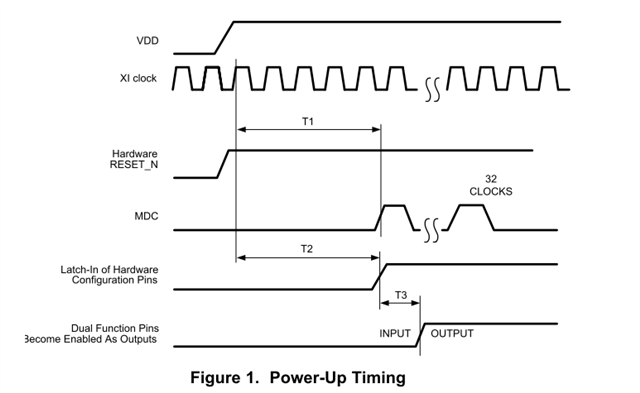
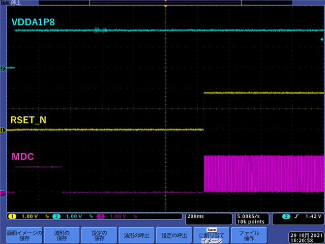
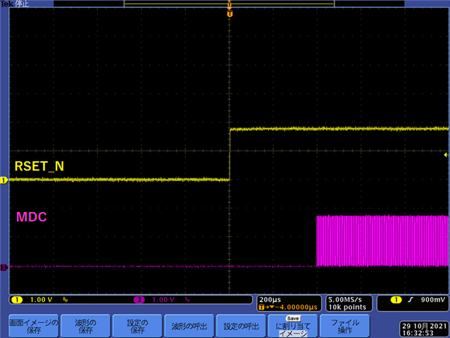
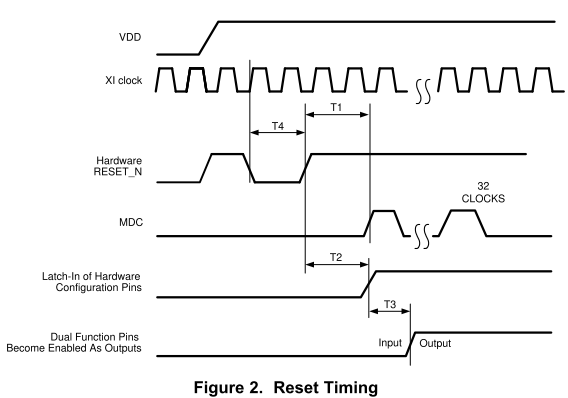
-They use reset sequence for strap setting.
We checked that during T2=120ns pins voltage remain the same voltage.
-RBIAS resistance is 11kohm±1%.
-They checked the same contents with MODE1, MODE3 and MODE4. However, it occurs only MODE2.
So, we understand that strap settings depend on voltate level and sequence only.
Furthermore, we recognize that we have to confirm pin voltage carefully.
If you have some advice for it, could you let us know?(Example, in case of MODE2, threshold level,,,)
(We also confirm any no errata for DP83867IS on Web.)
Kind regards,
Hirotaka Matsumoto