This thread has been locked.

If you have a related question, please click the "Ask a related question" button in the top right corner. The newly created question will be automatically linked to this question.

TCA9803: An error happend at EMI test

Part Number: TCA9803

Dear Specialists,

My customer is encountering transmission error at EMC test.

I would be grateful if you could advise.

---

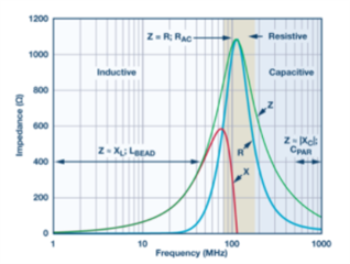
TCA9803DGKR has a problem in the EMC test.

In the radiation immunity test, I2C error occurs when irradiating an electromagnetic wave of 10V / m at a frequency of about 80 to 100MHz.

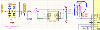
The circuit is attached PowerPoint. This connection was suggested by E2E.

TCA9803 connection diagram.pptx

The wiring distance between TCA9803s is roughly 30 cm to 50 cm.

The distance between TCA9803 to BUS MASTER and TCA9803 to SLAVE is within 10 cm.

I think that the wiring distance is long and it is affected by noise.

Could you please provide how to improve.

Is it better to use Pull Up or Pull Down at the receiving end when the transmitting distance is long?

---

I appreciate your great help in advance.

Best regards,

Shinichi

  • Hi Shinichi,

    I am reviewing this over with an I2C expert. I'll get answer to you by tomorrow at 5pm CT. 

    Regards,

    Tyler

  • Hi Shinichi,

    The schematic looks good to me, and seems to follow the correct wiring for A and B sides of the device. 

    I would assume since the wire distance is quite long ==> 30cm to 50cm, and the distance between Bus Controller and Bus Target is <10cm, that there would be electromagnetic noise coupled onto these lines that would cause I2C bit errors in communication. If you are injecting a wave at 100MHz, the wavelength is 3m, quarter wavelength = 0.75m. Since the wiring is max 0.5m, you are getting close to this quarter wavelength mark, which makes the wire act like a fairly good antennae to pick up this 10 V / m wave. It wouldn't surprise me if you shorten the wiring somehow, you might have better signal integrity. I2C is usually inter-board connections, and the wiring distance is quite short, giving it a better rejection ratio against EMI. 

    Increasing the value of the pullup resistors would hold up the voltage better and help with fighting off EMI. We are limited in this case because I2C has specific rise time standards as well as specific voltage level requirements. 

    Filtering on the power supply might help this situation too, since the wave might be coupling onto the supply as well. It wouldn't hurt to put a few filter caps from VCC to GND there. 

    Are you using shielded cabling? 

    Can you send pictures/captures of the failure waveforms you are injecting into the system?

    Regards,

    Tyler

  • Hi Tyler,

    Thank you for your reply.

    I understand that it is affected because the transmission distance of I2C is long and it is close to 1/4 wavelength of the frequency of EMI noise.

    I'll ask the customer to confirm the increase in the pull-up resistance value and the countermeasures for the power supply.
    Also I'll ask them to get the waveform as well.

    Transmission does not use cables. It is connected by multiple boards via a connector.
    At the customer's site, various measures were taken on the pattern, but they were ineffective.
    Is there any other pair that can be done on the board?

    ---The customer's comment

    There is also a GND guard between SDA and SCL to prevent crosstalk.
    However, the radiation immunity still causes a communication error near 90MHz.

    It was said that PDR and PUR were NG on the B side, so only Capacitor was added between SDA-GND and SCL-GND.
    I tried various things such as inserting and inserting ferrite beads today, but it did not improve at all. .. ..

    ---

    I appreciate your great help and cooperation.

    Best regards,

    Shinichi

  • Hi Shinichi,

    I think the long length of cable is the main issue here when testing EMI. Yes, see how increasing pull-up affects the test. Filter on supply voltage to eliminate noise on supply lines.

    I am confused on what exactly you are talking about when you say:

    Transmission does not use cables. It is connected by multiple boards via a connector.
    At the customer's site, various measures were taken on the pattern, but they were ineffective.
    Is there any other pair that can be done on the board?

    The wiring distance is the length of inter-board connections --- trace length? So I am assuming shield-cabling is not an option. What pattern? What do you mean by any other pair that can be done on the board?

    I may have misspoke when talking about having pull-up/down resistors on the receiving end. Unfortunately for this device it is incorrect to have PUR/PDR on the B-side due to the current source that helps to determine whether the bus is driving low. The customer's current circuit configuration is being used correctly without PUR/PDR on the B-side.

    What is the value of the capacitor to ground on both the SDA and SCL lines? What signal rate is the customer operating at in I2C? Too much bus capacitance can affect the transmission rise time on the SDA and SCL lines of an I2C bus causing communication errors. How many controller/target devices are on the I2C bus?

    Do we know the electrical characteristics of the ferrite beads used? Like a curve as such:

    Regards,

    Tyler

  • Hi Tyler,

    Thank you for your reply.

    Is there any other pair that can be done on the board?

    --->This is a typo. I was going to ask if there were any other measures.

    The customer and I understand PUR or PDR of B side is not recommended.

    The used ferrite beads are 742792040.

    742792040-1720361.pdf

    When they were installed near the device, they were no effect.

    As new information, when the customer connected the cable to the connector near the middle of the transmission line and made the ferrite core make three turns,

    normal communication became possible.

    It is speculated that placing the ferrite core near the midpoint of transmission may have been successful.

    So, they are considering using ferrite beads at the middle point as a countermeasure. Is this direction correct?

    It is known that the noise suppression effect is improved when the filter is composed of ferrite beads and a capacitor.

    We are thinking it is difficult to add a capacitor because 20 devices are connected to the I2C line and there is a capacitance constraint (<400pF) on the B side of the TCA9803.

    I appreciate your great help and cooperation.

    Best regards,

    Shinichi

  • Hi Shinichi,

    Looks like the ferrite bead is attenuating the correct range of frequencies as per the datasheet. The 80MHz - 100MHz range seems to be in the resistive region of the ferrite bead as per the datasheet. 

    I figure that connecting near the middle of the transmission probably helped to reduce the antennae affects that I described previously. I think it is a good idea to implement the ferrite beads at the middle point. The capacitance on the other hand is tricky. TCA9803 follows I2C standards for bus capacitance which is standardized at <400pF. If you plan on adding more capacitance, keep in mind trace capacitance from the PCB, # of devices connected to the bus, signal rate, pullup resistance value, etc. An I2C buffer solution might be helpful in resetting bus capacitance if the design is nearing the 400pF limit. 

    Do you have schematic that has more detail than the attached power point? Do you have scope captures of I2C data streams before and after implementing the middle connection?  

    Regards,

    Tyler

  • Hi Tyler,

    Thank you for your reply.

    In this case, it is effective to install the ferrite core near the middle of the transmission line.

    So, Ferrite beads will be installed on the substrate for confirmation.

    On the other hand, I2C must have a capacitance value of 400pF or less.

    For this reason, we will limit it to limited use.

    I appreciate your great help and cooperation.

    I'll try to obtain the waveform and schematic.

    Best regards,

    Shinichi

  • Hi Tyler,

    I could obtain the schematic and waveform.

    Could you please advise.

    Master Side

    Slave Side

    WURTH FB (742792040) was put in one by one near the middle of all the lines of power supply, GND, SDA, SCA.

    0.1uF ceramic capacitors are attached to both sides of the FB so that the distance between the power supply and GND is π type.

    SDA and SCL lines are FB only. (It feels like the noise is attenuated only by stray capacitance)

    The waveform with Chip Ferrite Beads measured at Slave Side 

    Before the hangup, communication is normal.

    EMI is radiated and communication is hung for 0.5s.

    After that, communication is successful.

    Communication was not possible before adding the ferrite beads.

    Yellow: SDA, Blue: SCL

    Measured with an oscilloscope with a 20MHz filter

    ---customer's comment---

    I2C errors have been eliminated by adding ferrite beads to SCL, SDL, power supply and GND near the middle of the transmission line.
    The error judgment inside the microcomputer was delayed so that the error disappeared.

    However, there is something strange about the waveform.
    There is a section where the SCL is always L for 0.5 seconds (so-called bus hang-up state).

    Radiation immunity noise occurs only twice, at the moment when application starts and at the moment when application ends.
    Communication can be continued normally while noise is being radiated (for the time being, about 20 seconds).
    Therefore, the pattern wiring length may be irrelevant.

    * It is not due to the I2C buffer. It was the same even if I removed the I2C buffer.

    I guessed like this.
    GND is
    ・ Steady state → Disturbed by noise → Is the I2C waveform disturbed for a moment? → Hang up?
    ・ Disturbed by noise → Return to steady state → Is the I2C waveform disturbed for a moment? → Hang up?
    Or something like that. .. .. The microcomputer may be weak.

    ---

    The customer has additional question, could you please advise.

    Do you think it is better to use Common Mode Filter?
    Common mode noise can be removed, but it is difficult to add CMF because it must be inserted between each line and GND.

    I appreciate your great help and cooperation.

    Best regards,

    Shinichi

  • Hi Tyler,

    The customer is thinking about adding series resistance in the SCL and ADL.

    Could you please advise. 

    ---

    I searched various online articles and there was information that if I put 100Ω or 330Ω in series with the SCL and SDA terminals of I2C, it would be more resistant to RF noise.

    Also Section 7.4 of the NXP I2C specification mentions series protection resistors.

    Does TCA9803DGKR have a regulation for the resistance value to be put in the series for SDA and SCL pins?
    Is there a regulation of the place to add?
    (For example, SCL is the closest to the SCLB on the MASTER side 9803? SDA is the closest to the pins of both MASTER and SLAVE?)

    I wanted to try this series resistance with inserting FB and C to improve the noise immunity.

    ---

    I appreciate your great help and cooperation.

    Best regards,

    Shinichi

  • Hi Shinichi,

    In this case, it is effective to install the ferrite core near the middle of the transmission line.

    So, Ferrite beads will be installed on the substrate for confirmation.

    I think this is a good solution. Installing ferrite core near the middle of transmission lines probably helps to eliminate reflections by reducing transmission line length. The ferrite bead has an approximate impedance of 300ohm 90MHz and 600ohm @ 100MHz , which is good for the EMI testing that is being conducted. 

    On the other hand, I2C must have a capacitance value of 400pF or less.

    For this reason, we will limit it to limited use.

    I forgot what device we looking at in this question. This is my bad. The TCA9803 is a I2C buffer. This device separates the bus capacitance from one side of the bus to the other. So theoretically, you could have double the amount of capacitance: 400pF on A side, 400pF on B side. This fact gives more design room concerning capacitance limitations due to I2C standards. 

    In the schematic for the slave/target side, I see that there are pullup resistors R7, and R6. I see that they are open, but these resistors should not be present on the B side even when the TCA9803 is not active: 

    It is recommended to leave the pins on the B-side floating if unused as per the datasheet:

    External pull-ups could potentially provide additional current pushing the IILC out of spec, preventing the bus from being able to transmit a logic LOW.

    * It is not due to the I2C buffer. It was the same even if I removed the I2C buffer.

    I think this makes sense because when the radiation immunity noise occurs, it doesn't seem to affect the SDA line. If it affected the TCA9803, I would assume it would affect both the SCL and SDA lines somewhat equally, latching both lines low, but this seems to only affect the clock line. 

    I noticed that there was some ESD protection on the bus lines on the B-side. There might be a possibility that there is some leakage current from the ESD diodes that could be pushing the IEXT-I / IEXT-O out of spec, see datasheet:

    I guessed like this.
    GND is
    ・ Steady state → Disturbed by noise → Is the I2C waveform disturbed for a moment? → Hang up?
    ・ Disturbed by noise → Return to steady state → Is the I2C waveform disturbed for a moment? → Hang up?
    Or something like that. .. .. The microcomputer may be weak.

    I don't know if I understand how this leads to the assumption of a weak microcomputer? 

    Do you think it is better to use Common Mode Filter?
    Common mode noise can be removed, but it is difficult to add CMF because it must be inserted between each line and GND.

    Not sure if common mode filter is a good option between each bus line and GND due to intricacy of implementation. First-order, second-order common mode filters may have an impact on bus rise time and bus capacitance due to the components of the filter. 

    Does TCA9803DGKR have a regulation for the resistance value to be put in the series for SDA and SCL pins?

    Section 9.4.1.1.2 of the datasheet talks about series resistance and its affects on the device:

    The main thing to remember about adding series resistance is that it will affect your Vol due to the voltage drop across the resistor. The value of the resistor must be chosen appropriately to make sure the voltage drop doesn't interfere with your logic levels. Also must keep in mind that adding a series resistor will create a low-pass filter with the bus capacitance of your SDA and SCL lines, which is another design consideration. 

    Regards,

    -Tyler

  • Hi Tyler,

    Thank you for your reply.

    I'll share your suggestions with the customer.

    When they have an additional question, I consult you again. 

    I appreciate your great help and cooperation.

    Best regards,

    Shinichi