A related question is a question created from another question. When the related question is created, it will be automatically linked to the original question.
If you have a related question, please click the "Ask a related question" button in the top right corner. The newly created question will be automatically linked to this question.
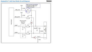
It seems that the signal output on the GPU is still through the DP Connector Pin13 CAD signal H or L, allowing the GPU to determine the output AUX or DDC signal and control the DDC_EN action