This thread has been locked.

If you have a related question, please click the "Ask a related question" button in the top right corner. The newly created question will be automatically linked to this question.

DS125DF1610: Ds125df1610 10G/1G Signal is not Link

Part Number: DS125DF1610
Other Parts Discussed in Thread: DS125MB203

Hi TI

     The hardware channels are as follows: backplane & LT;=> Ds125df1610 & lt;=> ds125mb203 <=> Panel 10 GBIT/s optical module.It can be configured through i2C channels DS125DF1610 and DS125MB203.

      The problem is: the signal from the backplane, whether it is 1G signal, or 10G XFI signal, the panel optical port is not link (self-loop and docking other devices, are not link) DS125DF1610 chip uses the default configuration of power-on, DS125MB203 uses the default value, DS125MB203 registers are as follows:

root@ebang:/$i2cdump -f -y 20 59

     0  1  2  3  4  5  6  7  8  9  a  b  c  d  e  f    0123456789abcdef

00: 08 00 00 00 00 00 10 01 00 00 ff 70 00 00 00 2f    ?.....??...p.../

10: ad 82 00 00 00 00 2f ad 82 00 00 00 00 2f ad 82    ??..../??..../??

20: 00 00 00 00 2f ad 82 00 0c 00 00 00 2f ad 82 00    ..../??.?.../??.

30: 00 00 00 2f ad 82 00 00 00 00 2f ad 82 00 00 00    .../??..../??...

40: 00 2f ad 82 00 00 38 00 05 00 00 00 00 00 00 00    ./??..8.?.......

50: 00 46 00 00 00 00 10 64 21 00 54 54 00 00 00 00    .F....?d!.TT....

60: 00 00 00 00 00 00 00 00 00 00 00 00 00 00 00 00    ................

70: 00 00 00 00 00 00 00 00 00 00 00 00 00 00 00 00    ................

80: 00 00 00 00 00 00 00 00 00 00 00 00 00 00 00 00    ................

90: 00 00 00 00 00 00 00 00 00 00 00 00 00 00 00 00    ................

a0: 00 00 00 00 00 00 00 00 00 00 00 00 00 00 00 00    ................

b0: 00 00 00 00 00 00 00 00 00 00 00 00 00 00 00 00    ................

c0: 00 00 00 00 00 00 00 00 00 00 00 00 00 00 00 00    ................

d0: 00 00 00 00 00 00 00 00 00 00 00 00 00 00 00 00    ................

e0: 00 00 00 00 00 00 00 00 00 00 00 00 00 00 00 00    ................

f0: 00 00 00 00 00 00 00 00 00 00 00 00 00 00 00 00    ................

root@ebang:/$^C

Question:

1. Ds125df1610 chip and DS125MB203, do you have pass-through mode or by-pass mode? Because there is no Link at present, I cannot locate the problem of DS125DF1610 chip or DS125MB203?

2. There are many registers in the DS125DF1610 chip. What registers should be configured for the 10G XFI signal from the backplane?

3. The default power-on configuration is used for the DS125DF1610 chip.Other values have been manually configured before, and do not link.

4. I also tried the PIN mode of DS125MB203, but it did not link.

5. Please provide the IBIS model files of DS125DF1610 and DS125MB203 chips.

DS125DF1610 branch card.pdf

  • Request noted. I will target to advise by close of business tomorrow (Thursday USA pacific time.)

    -Rodrigo Natal

  • Hi,

    Could you provide estimates of how much insertion loss the channels in your system have?

    1. Ds125df1610 chip and DS125MB203, do you have pass-through mode or by-pass mode? Because there is no Link at present, I cannot locate the problem of DS125DF1610 chip or DS125MB203?

    You can bypass the CDR block of the DS125DF1610 and output raw data instead of retimed data.  This can be done with the following writes.

    Register Address Write Value Write Mask Description
    Select Appropriate Device Channel
    0x1E 0x00 0xE0 Select Raw Data
    0x09 0x20 0x20 Override MUX setting

    There is no bypass mode on the DS125MB203, but you can reduce the EQ and de-emphasis to minimize the effect the device will have in the signal chain.

    2. There are many registers in the DS125DF1610 chip. What registers should be configured for the 10G XFI signal from the backplane?

    The key settings of this device can be broken down into receiver settings, CDR settings, and transmitter settings.  I would start with ensuring that you can get CDR lock and that the device measures a reasonable HEO/VEO.  Depending on your insertion loss, you may want to configure the device to use adapt mode 1 or 2 instead of adapt mode 0 so that the device receiver automatically adapts the CTLE and DFE settings.

    CDR Settings:

    Register Address Write Value Write Mask Description
    Select Appropriate Device Channel
    0x2F 0xB0 0xF0 Set CDR to lock to 10.3125 Gbps
    0x0A 0x0C 0x0C Assert CDR Reset
    0x0A 0x00 0x0C Release CDR Reset

    Receiver Settings:

    Adapt mode can be adjusted through channel register 0x31[6:5].  After configuring this, it is recommended to assert and release CDR reset (as detailed above) in order to start the adaptation process.

    You can use the eye opening monitor to evaluate the effectiveness of the receiver settings.

    Transmitter Settings:

    FIR settings are adjustable through channel registers 0x3D-0x3F.  The VOD can be adjusted through the drv_sel_vod setting, which is split between register 0x0D and 0x2D.

    5. Please provide the IBIS model files of DS125DF1610 and DS125MB203 chips.

    Please complete and submit the request forms that are on the product pages for each of those devices.

    Thanks,

    Drew

  • at the present, through your advice above, 1G mode is link up.but 10G mode isn't link up yet.   I set  0x2f to 0xb6,then 1G is link up.  Could you give me some advices on the issues of  10G mode no linking up. looking forward to your reply.thank you.

  • Hi,

    I would recommend taking a look at channel register 0x01 on the DS125DF1610.  This has some status indicators that can be helpful to determine where a link issue is occurring.

    Thanks,

    Drew

  • the value of address 0x01 is 0x80. On the other hand, there is a situation that i link is very confused : on the same date path, when i use a 1G optical  module ,the link is up; but i pull out the 1G optical module and plug a 10G optical module, then the link is down.  you know ,this situation doesn't  happen in my other  type devices. for this situation,and 10G optical module  should be  compatible to 1G mode. so i think that after change 1G optical module to 10G optical module, link is also up with any software changing.Could you give me some advices on the 10G no linking issue? my data path is like this : backplane <->DS125DF1610<->DS125MB203 <-> optical  module .looking forward to your reply,thanks very much!

  • See my inputs below.

    Related to: "on the same date path, when i use a 1G optical  module ,the link is up; but i pull out the 1G optical module and plug a 10G optical module, then the link is down"

    • Question: Could you provide a full retimer channel registers dump both for the 1G case where link is up and also the 10G case where link is down

    my data path is like this : backplane <->DS125DF1610<->DS125MB203 <-> optical  module 

    • Please provide a setup block diagram along with estimates for insertion loss in dB for each of the link segments. This info is important for troubleshooting

    Thanks,

    Rodrigo Natal

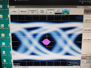
  • Above, it is the eye diagram picture. thank you for your timely reply! i'll provide register dump values for you. but now i have a confused question about "DATA RATES" for "FIRST GROUP DIVIDER" and "SECOND GROUP DIVIDER". As you know, when i set 0x2f to 0xb6, the 1G optical module links up. the value 0xb6, means "10.3125, 1.25" and  the rate for "FIRST GROUP DIVIDER" and "SECOND GROUP DIVIDER" is 8:1 . the number 8 means 10.3125G, the number 1  means 1.25G?  my question is that 8:1 and 10.3125, 1.25 is the cause of 1G linkup ,and 8:1 and 10.3125, 1.25 only is ok for  1G optical modules . Does you agree with me in this opinion? if i want to use 10G optical module, what value  i shoud to set for the "FIRST GROUP DIVIDER" and "SECOND GROUP DIVIDER"? and Could you tell me the defference of  "FIRST GROUP DIVIDER" and "SECOND GROUP DIVIDER"? and what do they means?looking forward to your reply.thank you.

  • Hi,

    Could you clarify where this eye diagram is taken in your system?

    Although it is not clear from the table in the datasheet, the first group divider of 8 actually matches with the 1.25 Gbps, and the second group divider of 1 matches with 10.3125 Gbps.  For locking to the first group, the VCO is set to 10 GHz, with a divider of 8.  For locking to the second group, the VCO is set to 10.3125 Gbps with a divider of 1.

    The group dividers that are set with 0x2F = 0xB6 should be appropriate for locking to a 1.25 Gbps signal and 10.3125 Gbps signal.

    Thanks,
    Drew

  • the eye diagram is taken from optical module'S tx .thanK you.

  • Could you give me the user's guide of the chip ds125df1610?thank you!

  •  and the user guide of DS125MB203.thank you.

  • and i did so many experiments.now i find that the eye diagram of optical 10G module'TX is not stable ,it is geting smaller as time is going ,at last it gets stable ,just like the eye diagram i gave you before. why? why eye diagram is changing , and sometimes it doesn't look like a eye, its so fuzzy, not clear at all. looking forward to your reply.thank you.

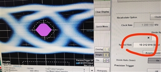
  • a new eye diagram. the key registers 's value such as:DEM ,drv_sel_vod,FIR(pre,main,post) is as follows: DEM is 0x2, drv_sel_vod is 31, pre FIR is 0, main FIR is 0x2e,post FIR is 0x20.adapte mode addr 0x31 is 0x60 and i have a question: if i set post FIR  to be nagative int , the eye diagram is ganna be worser, if i set post FIR  to be postive int ,such as 0x20,the eye diagram is ganna be clearer.as you know, through the chip datasheet ,the post FIR should not be a postive int and should be a negative value. how to explain the situation? and above eye diagram,you look at the red circle, the clock is 10 312 816 K, but no 10 312 5xx K. from the defferent of this clock, Could you give some advices for 10G link? thank you sincerely!

  • Hi,

    It sounds like you are applying a lot of post-cursor attenuation in order to observe a good eye.  What is the equalization of the DS125MB203 set to?  Can you provide estimated loss for the various connections in your block diagram?  This will help us better understand your system.

    Regarding user's guides, you can find technical documentation for both of these parts on their respective product pages.  They both have an EVM user's guide.  Additionally, you may find our 10G retimer programming guide (linked below) helpful.  Although it is not an exact match for DS125DF1610, many of the register writes are the same and it can prove valuable if you verify that the register writes match the register map in the DS125DF1610 data sheet.

    https://www.ti.com/lit/pdf/snla323

    Thanks,

    Drew

  • first ,thank you for your timely reply!  second,i'll tell you my last debugging progress and results, i have 4 ports'10G and 1G are  linking up. other optical modules are linking down and i am tring defferent register values .  i analysized the reason of 1G linking up,  the register addr 0x6[3]  of DS125MB203 should been set 1,not 0 , otherwise, the values in those registers do not work.  regarding 10G linking up,i think i reach the target because i set the adapt mode,vod,dem,fir of DS125DF1610 and EQ, vod,dem,RXDET of DS125MB203 . and i found a phenomenon : my device consits of eight optical modules in each slot, and have 8 slots in total, so as you know, one  of 8 optical modules connects with defferent DS125MB203 and  DS125DF1610, so i must to try and configure defferent register values to get it link up.  8 slots * 8/per slot=64 optical modules . in other words ,i need to prepare 64 parameter sets to configure  the all optical modules, my god, it's so crazy.  and regarding "Can you provide estimated loss for the various connections in your block diagram?" this request, i don't understand you, how can i  get the loss data of my device?oscillascope? looking forward to your reply.thank you.

    attenuation
  • Hi,

    Can you provide estimated loss for the various connections in your block diagram?

    We are interested in the attenuation that your PCB has.  This gives perspective as to how much equalization needs to be provided by the DS125MB203 and DS125DF1610.

    Thanks,

    Drew