Part Number: TUSB7340
Hi Team,
Can you help me answer a question about the drive level supported by XI/XO pins on TUSB7340?
My understanding is that the drive level is defined by the crystal, not the device.
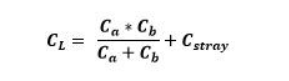
As long as the load capacitance and ESR are within the datasheet spec our device should be able to operate with the crystal, correct?
However, how do customers calculate the maximum drive level seen by the crystal based on the values we provide in the datasheet and their chosen load capacitance/recommended 2MOhm shunt resistor?
Based on the following other thread, it looks like the answer is to confirm with crystal vendor that it can be driven by 1.8V clock and the board design and layout guideline file implies the same, but I'd like to confirm.
e2e.ti.com/.../tusb4020bi-drive-level-spec-of-tusb4020bi
Thank You,
Jacob Butler