This thread has been locked.

If you have a related question, please click the "Ask a related question" button in the top right corner. The newly created question will be automatically linked to this question.

DS90UB948-Q1: DS90UB948-Q1 generate pattern

Part Number: DS90UB948-Q1
Other Parts Discussed in Thread: ALP, USB2ANY

Hi

I am now troubleshooting which part of the video output has a problem. SER:941 DES:948 Now I want to output pattern from 948. My configuration is as follows:

WriteOfI2c_Byte(UB948,0x49,0x80);//SET MODE_SEL0

WriteOfI2c_Byte(UB948,0x1D0x05);
WriteOfI2c_Byte(UB948,0x1E,0x55);


WriteOfI2c_Byte(UB948,0x66,0x03);  //enable PGCDC1
WriteOfI2c_Byte(UB948,0x67,0x03);  //66.6M pclock

//H V  1920*480
WriteOfI2c_Byte(UB948,0x66, 0x07);  
WriteOfI2c_Byte(UB948,0x67,0x80);  
WriteOfI2c_Byte(UB948,0x66,0x08);
WriteOfI2c_Byte(UB948,0x67,0x07);
WriteOfI2c_Byte(UB948,0x66,0x09);
WriteOfI2c_Byte(UB948,0x67,0x1E);

//H V TOTAL   1938*570
WriteOfI2c_Byte(UB948,0x66,0x04);
WriteOfI2c_Byte(UB948,0x67, 0x92);
WriteOfI2c_Byte(UB948,0x66,0x05);
WriteOfI2c_Byte(UB948,0x67,0xA7);
WriteOfI2c_Byte(UB948,0x66,0x06);
WriteOfI2c_Byte(UB948,0x67,0x23);

//HBP: 14
WriteOfI2c_Byte(UB948,0x66,0x0C);
WriteOfI2c_Byte(UB948,0x67,0x0E);

//VBP: 6
WriteOfI2c_Byte(UB948,0x66,0x0D);
WriteOfI2c_Byte(UB948,0x67,0x06);

//H SYNC 13
WriteOfI2c_Byte(UB948,0x66,0x0A);
WriteOfI2c_Byte(UB948,0x67,0x0D);

//V SYNC 6
WriteOfI2c_Byte(UB948,0x66,0x0B);
WriteOfI2c_Byte(UB948,0x67,0x06);


WriteOfI2c_Byte(UB948,0x66,0x0E);//enable PBSC 
WriteOfI2c_Byte(UB948,0x67, 0x03);  /set  negtive
WriteOfI2c_Byte(UB948,0x65,0x03);  //enable 24bit and internal clock
WriteOfI2c_Byte(UB948,0x64,0x11);  //enable pattern generator

I write 941's 0x01 register WriteOfI2c_Byte(UB941, 0x01, 0X08); to close 941's dsi. Make sure not to affect the 948 output pattern.
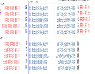
but The latter lvds to mipi signal chip cannot recognize the lvds signal and the clock detected by the two signals is 16468, which should be 32300.

 what's the problem? Are there any other registers that are not configured?Or my thinking is wrong?

thanks
  • Hello, 

    I will look into the information provided. Do you happen to have access to a USB2ANY device and utilize our ALP GUI? This will help with using patgen on the deserializer. 

    Best,

    Shu

  • Hi,

    Unfortunately, We don't have USB2ANY, and there is no related interface in the schematic.

    Best

    Luuel

  • Hi Luuel, 

    What are the strap modes for this set up? I cannot tell from the attached schematic. 

    I looked over the configuration sequence and those are the correct steps. I did notice something in your timings, can you double check those? 

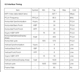
    you stated that H V TOTAL  1938*570 but just looking over the HBP and HSYNC parameters, they add up to much greater than that. 

    These are the equations needed to calculate the timings for either horizontal or vertical timings. 

    Total Pixel = Active + Blanking 

    Blanking = Front porch + back porch + sync width 

    Based on the HBP of 14 and HSYNC of 13 and assuming HFP is 0, the total horizontal should 1947 instead 1938. 

    Best,

    Shu

  • Hi,Shu

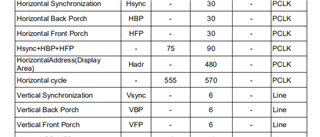
    The first picture I provide is the typ value of the timing setting for the display I am using. We use this set of timing for soc, soc->display verification can be displayed.
    The soc->941->948->lt9211-> display screen we are currently using shows abnormality. I am excluding which part is the problem. The lt9211 output pattern is correct.
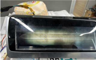
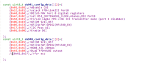
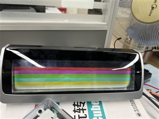
    I transplanted the above configuration to the 941, but still can't output correctly, it seems that there is a problem with the internal clock. I use the external dsi+ current configuration to display color bars, but the display effect is still not good, as shown below
    I guess there is a timing problem with my dsi? So I want to use the internal generated graphics of 941 or 948 directly without external dsi input to verify.
    The problem I am having now is that there is something wrong with my internal clock settings I have tried writing 0x04 to the 0x65 register
    But the 948 terminal can't output the lvds signal, and I can't seem to change the output clock even by modifying the "N" value.

  • dsi+ configuration above, but what I want now is the internal graphics output entirely from the 941 or 948。

    Best,

    Luuel

  • Hi Luuel, 

    I understand what you are trying to test and also agree that just using the 948 to generate the graphics is the best approach at this moment. 

    What are the strap modes for this set up? I cannot tell from the attached schematic. 

    Can you provide this information? If the 948 patgen is done correctly and still not able to output display, we need to check the MAP_SEL configuration and match it to what the display has specified. Can you send me the MODE_SEL0 setting and the display datasheet?

    Best,

    Shu

  • Hi,Shu

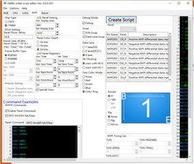
    The screenshot is a generic configuration of my 941 and 948. Attached is display datasheet。

    Best,

    Luuel

  • Hi Luuel, 

    I have some questions

    The latter lvds to mipi signal chip cannot recognize the lvds signal and the clock detected by the two signals is 16468, which should be 32300.

    How is this lock detected and where are you measuring this signal? The 16468 rate is approximately half of the expected rate. This might not be a coincidence and correlate to the dual LVDS to single MIPI converter. 

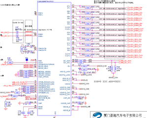
    Can you share the full schematic between the 948 -> LT9211 -> LCD?

    But the 948 terminal can't output the lvds signal

    When you are just using the 948 to try and generate graphics, how is this LVDS signal measured? right out of the 948 before going into LT9211? 

    Also are there any programming being done to the LT9211? If so, can you share those configurations? 

    Best,

    Shu

  • Hi Shu,

    OK, I'll just chat to you. The 948 output lvds signal is directly connected to the 9211 after a 100Ω resistor. I can measure the signal waveform through this resistor, and I can also judge whether there is an lvds signal through the data read from the read-only register inside the 9211. I confirmed with an oscilloscope that there is no lvds output. The configuration of 9211 is just to initialize the chip, and then judge the current state by reading the register. I re-authenticated this morning and it seems to have found the reason. If I write the 0x65 register as 0x04 the following i2c cannot be written correctly. If I write the 0x65 register as 0x03, it is the above 16468 without lvds output and the clock cannot be changed. But 0x65[2] is to be set to 1 according to the description.This problem is very strange, how to solve it

    Best,

    Luuel

  • Hi Luuel, 

    Can you change following to be 0x02? The internal oscillator frequency for the 948 is actually 140MHz, not the same as the 200MHz like the 941. This could be a part of the issue. 

    WriteOfI2c_Byte(UB948,0x67,0x03);  //66.6M pclock

    I am going to do some testing on my side for the 948 using our Analog Launch Pad SW tool to generate pattern output and compare register settings with you. 

    Best,

    Shu

  • Hi Shu,

    Thank you very much, when can you provide me with the register configuration?

    Best

    Luuel

  • Hi Luuel, 

    I hope to provide the register configuration by the end of this week. 

    Best,

    Shu

  • Hi Luuel, 

    Can you try the 948 patgen with these register settings? The first section is the Patgen registers, programmed using the indirect register indexing 0x66/0x67. The second section is the main page register settings, used to enable patgen setting after selecting internal clock. 


    Patgen Reg   Data Name
    0x0000          0x00 PGRS
    0x0001          0x00 PGGS
    0x0002          0x00 PGBS
    0x0003          0x02 PGCDC1
    0x0004          0x92 PGTFS1
    0x0005          0xA7 PGTFS2
    0x0006          0x23 PCTFS3
    0x0007          0x80 PGAFS1
    0x0008          0x07 PGAFS2
    0x0009          0x1E PGAFS3
    0x000A          0x06 PGHSW
    0x000B          0x1E PGVSW
    0x000C          0x06 PGHBP
    0x000D          0x1E PGVBP
    0x000E          0x03 PBSC
    0x000F          0x1E PGFT
    0x0010          0x0E PGTSC
    0x0011          0x21 PGTSO1
    0x0012          0x43 PGTSO2
    0x0013          0x65 PGTSO3
    0x0014          0x87 PGTSO4
    0x0015          0xA9 PGTSO5
    0x0016          0xCB PGTSO6
    0x0017          0xED PGTSO7
    0x0018          0x0F PGTSO8
    0x0019          0x00 PGBE
    0x001A          0x01 PGCDC2

    Register         Data Name
    0x0064          0x15 PGCTL
    0x0065          0x04 PGCFG

    Best,

    Shu

  • Hi,Shu

    Is the waveform of your 948 output similar to this? The video is my quick measurement of 10 outputs of the 948. Is this an lvds waveform?

    Best,

    Luuel

  • Hi Luuel, 

    Can you zoom out on the timescale of the capture so we can see all the outputs next to each other? 

    Best,

    Shu

  • Hi,Shu

    After reducing the captured time scale, the waveform is as shown below. Can you provide the waveform of the pattern generated by the 941? I write 0x35/0x45/0x55/0xE5 to the 0x64 register are all this waveform. Can you help me configure the RGB image to loop at 1 second intervals?

    Best,

    Luuel

  • Hi Luuel, 

    Since today is a US holiday for TI, we will resume activity on Monday 4/18. Thanks for your patience. 

    Regards, 

    Logan

  • Hi Luuel, 

    I will set up a 941 patgen configuration and get back to you with the results. 

    Best,

    Shu

  • Hi,shu

    Thank you, is the last configuration wrong here. The 0X0A register should be written to 1E, and the 0X0B register should be written to 0X06?

    Best,

    Luuel

  • Hi Luuel, 

    I looked over the display specifications and noticed that the active horizontal is 480 and active vertical is 1920. The below are the updated patgen register values. Can you try this again and let me know if anything changes on the display/output?

    Best,

    Shu

    Register Data Name
    0x0000 0x00 PGRS
    0x0001 0x00 PGGS
    0x0002 0x00 PGBS
    0x0003 0x02 PGCDC1
    0x0004 0x3A PGTFS1
    0x0005 0x22 PGTFS2
    0x0006 0x79 PCTFS3
    0x0007 0xE0 PGAFS1
    0x0008 0x01 PGAFS2
    0x0009 0x78 PGAFS3
    0x000A 0x1E PGHSW
    0x000B 0x06 PGVSW
    0x000C 0x1E PGHBP
    0x000D 0x06 PGVBP
    0x000E 0x00 PBSC
    0x000F 0x1E PGFT
    0x0010 0x01 PGTSC
    0x0011 0x21 PGTSO1
    0x0012 0x43 PGTSO2
    0x0013 0x65 PGTSO3
    0x0014 0x87 PGTSO4
    0x0015 0x89 PGTSO5
    0x0016 0xC9 PGTSO6
    0x0017 0xED PGTSO7
    0x0018 0x0F PGTSO8
    0x0019 0x00 PGBE
    0x001A 0x01 PGCDC2

  • Hi,Shu

    The results of the test are as follows:
    1. External video signal +941pattern config


    2. External video signal

    3.948 pattern config
       No video output


    Is the output image now the same as what you set?
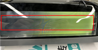
    At present, a very strange phenomenon occurs. When there is only an external video signal, the display will appear stripes in the red frame. I tried to restore the config of 941pattern to the default value, the stripe still exists, how can I make this stripe disappear?

    Best,

    Luuel

  • Hi Luuel,

    The 941 patgen shows correct behavior of the color bar and helps confirm the display is working properly. I believe the focus now is the link between the SOC and the 941. 

    What are the scopes in the video showing? Can you share the configuration of the external video going into the 941? If 941 patgen works, it is most like the timing going the 941 that is not being reconstruction properly. 

    Best,

    Shu

  • Hi,Shu

    Attached is the video of the soc output and the soc configuration. It should be RGB image + black and white. The one-pixel vertical bar on the right side of the display in the video appears to be correct, and the rest of the display appears to be covered in black. In addition, the color bars output by the 941 will also become dim at the back. Is there any command for 941 and 948 to restore all state to default?

    Best,

    Luuel

  • Luuel,

    We have a detailed guide on step by step how to design/debug DSI with 941AS here: https://www.ti.com/lit/pdf/snla356 

    Can you please read through this app note and then follow the steps in figure 3-2 to let us know where exactly things are going wrong?

    Best Regards,

    Casey