This thread has been locked.

If you have a related question, please click the "Ask a related question" button in the top right corner. The newly created question will be automatically linked to this question.

DS26LV31T: Driver output impedance data

Part Number: DS26LV31T
Other Parts Discussed in Thread: STRIKE, THVD1449V, THVD1449, THVD1428, THVD1429

Hi.

I have to protect against lightning and interferences a telemetry line RS422 which uses a DS26LV31T as driver. Therefore I would like a model of the three state Output Buffer to carry out Spice Simulations attacking the driver output with waveforms about 250 V and 10 A:

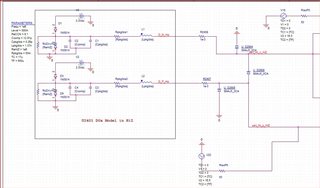
1- I have tried the Ibis model but the results  don´t convince me because it doesn’t include the ESD  clamping diodes. I´ve developed a model by advice of other designers that you can see in file Capture1, do you think is a proper model for the outputs, let´s say pins 2 &3? Can you provide me a model of the output driver impedance?

2- Could you tell me the output impedance when the driver is in high impedance and in normal operation? (I mean, an average).

3-I don´t understand the maximum rating of the Driver Output Voltage, it´s written in the datasheet (Power Off:D0+, D0-), what is the meaning of (Power Off:D0+, D0-)? Is differential, single ended  or what? Is the same maximum rating when the device is powered at 3.3 V.

4-Last but not least, I have to apply  waveforms that are mainly pulses or damped sinusoids, if the maximum ratings are exceed for a time let´s say 30 uS, how I could asses if the driver has survived the lightning/ interference? (See pdf file attached) .

DS26AN~1 (002).pdf

  • Hi Luis,

    1. There isn't an ESD diode to VCC on any of the DOUT pins. This is shown in the datasheet since DOUT (DO+/DO-) pins can handle voltage at power down  (according too abs max table this is from -0.5V to 7V when power down) - if there was an ESD diode to VCC on these pins it wouldn't be able to hit this specification. We don't have a public facing model to share for this part.

    2. This isn't a value we have spec'd. The closest thing you can look at is the input leakage current in tri-state (I_OZ) and use that to estimate the resistance using the typical leakage value (as this is at room temp and temperature related leakage will be lower at this point). 

    3. The spec is written to be read in two ways. The first is that there is no "normal operating max/min voltage" as it is assumed this is an output pin and the device will not output damaging signals to itself on these pins - this part wasn't necessarily built with the idea that external voltage surges will hit this pin. The second is that when VCC = 0V  DO+ w.r.t. ground or DO- w.r.t. ground must stay in-between -0.5V to 7V to prevent damage on device. 

    4. The model will not "break" when exposed and it will not show when damage will occur. If the part has its max ratings violated damage can occur - it is not recommended to to violate abs max as these are the ratings we do not guarantee the device will survive impact.  

    Best,

    Parker Dodson

  • Hi Parker,

    Thanks for your help. I have a couple of questions more:

    1- Do you know if TI has any circuit devoted to surge/lightning protection? Protection against conducted susceptibility/electromanegnetic interferences?

  • Sorry, I haven´t included the 2nd question and I pressed the button too soon.

    2-My analyis must be done with the equipment powered on, last attempt before giving up, could you provide me a ball-park idea of voltage maximum rating of Dx output when the driver is powered on?

  • Hi Luis,

    For your first question - We have some surge protected Transceivers (so TX and RX in one package) but not in the architecture that you are using. It will be more similar to devices like the THVD1449V which is a half duplex 1 channel transceiver with 4kV IEC surge protection so I am not sure if it will be able to withstand a lighting strike but that is really where the integrated surge would be maxed out for our parts (4kV Surge), it is RS-485 but it could possibly work in the application - other than that external surge diodes would have to help shunt the rest of the energy - is there any flexibility in the design or does it need to be a quad driver?

    For your second question: the safest bet is to design around the "off" value of a minimum of -0.5V w.r.t. ground and a max of 7V w.r.t. ground - this is due to the RS-422 standard expecting between 0V and 6V w.r.t. ground for these pins output voltages - this is the safest option because while operational max voltage may be higher we don't have the data to confirm that and the abs max is a bit over what is expected at runtime.

    Please let me know if you are opening to possibly look at other architectures that could provide a higher integrated surge protection - if not I'd look for a protection circuit that will shunt the harmful voltages and currents away from the IC in case of surge. 

    Best,

    Parker Dodson 

  • Is there any flexibility in the design or does it need to be a quad driver?Well, right now the project is ongoing, but for the future as a evolution

  • Sorry Parker, I had forgotten to log in, I was saying that for the future it could be useful any information that you provide me about surge protected transceivers as we need just one driver (see file attached). The design could be changed according to my surge protection analyisis in the current design.

    Of course, I am open to changes in the design because the initial design in my opinion it was too optimistic. Righ now, we use one driver and four receivers.

  • Hi Luis,

    So based on the schematic - I definitely think moving towards a surge protected device is possible - UART signals work well with RS-485 so the slight change in interface (RS-422 to RS-485) probably isn't much of an issue.

    At 3.3V we have the following surge protected parts - they are all 1 channel half duplex transceivers (so they can be either in TX or RX mode) - The biggest possibly issue I forsee with our surge protected parts is that they are slower than this driver (this driver has a max of ~30Mbps where as our surge protected line vary from 250kbps to 20Mbps, generally for UART the surge protected. I have listed only devices with 12Mbps or above to as the ones below 12Mbps are at 250Kbps which is well under max UART speeds.

    THVD1449V - 12Mbps, 4-kV IEC surge protection with separate logic power supply pin

    THVD1449 -- Same as above without separate logic supply pins (VCC is logic power supply)

    THVD1428 - 20Mbps - 3kV IEC surge protection

    THVD1429 - 20Mbps - 2.5kV IEC surge protection.

    These four devices would be best suited for your application as they have integrated surge - once again external protection may also still need to be added but these parts are some of our best parts for surge protection while still meeting your application goals. The best ones would be our newest ones the THVD1449 and THVD1449V.

    Please let me know you have any other questions!

    Best,

    Parker Dodson