This thread has been locked.

If you have a related question, please click the "Ask a related question" button in the top right corner. The newly created question will be automatically linked to this question.

TMDS181: cascading retimer

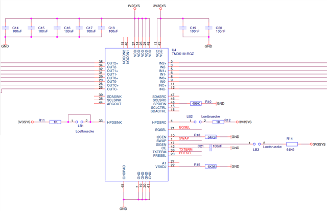
Part Number: TMDS181


Hi Team, 

can you please help with the topic below: 

We are a manufacturer of digital training systems by means of uncompressed video transmission to numerous participants in a room in real time. It is not uncommon for the video signal to have to be transmitted over longer distances.

For this reason, we have chosen to further develop new 4K-capable products when choosing a retimer for your TMDS181. So far, we are very satisfied with the performance of this component in our first prototypes.

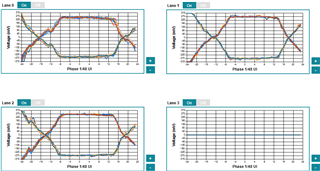
However, we noticed during the cascading of several retimers that the image signal becomes unstable and has sporadic dropouts. As a result, posts in official TI forums may be due to a jitter that is growing increasingly from retimer to retimer.


To be able to analyze this in more detail, our hardware developer would like to read it out using I²C and evaluate the EyeDiagram. Among other things, this is generated by parameters, which can only be found in an extended data sheet/manual according to the TI Forum. In addition to register bank 0 , the register bank 1 ( > HX20 registers) of the parameterization I²C bus is to be explained, which is not included in the free downloadable data sheet.


We would be very pleased if you could support us in this, in order to realize your product in cascades.

  • Jan

    Do they have a scope that can probe the TMDS181 output signal quality to debug this issue? If would be good if they can compare the output signal quality between a single TMDS181 and cascading TMDS181 implementation.

    Can they also try the follow I2C write to the TMDS181 registers and see if it helps? 

    <aardvark>

    <configure i2c="1" spi="1" gpio="0" tpower="1" pullups="0"/>

    <i2c_bitrate khz="100"/>

    <i2c_write addr="0x5e" count="1" radix="16">09 06</i2c_write> <sleep ms="10"/>   -> Set lane and polarity swap, disable automatically power down base on HDP_SNK

    <i2c_write addr="0x5e" count="1" radix="16">FF 01</i2c_write> <sleep ms="10"/> -> Select Page 1 registers

    <i2c_write addr="0x5e" count="1" radix="16">01 01</i2c_write> <sleep ms="10"/> -> Charge pump enable. PLL mode, used with the HDMI

    <i2c_write addr="0x5e" count="1" radix="16">02 3F</i2c_write> <sleep ms="10"/>  -> Charge pump current control. 7F max charge pump current setting, may need to sweep the value

    <i2c_write addr="0x5e" count="1" radix="16">00 03</i2c_write> <sleep ms="10"/> -> Bit 0 -> Enable PLL and Bit 1 -> Enable bandgap

    <i2c_write addr="0x5e" count="1" radix="16">0B 33</i2c_write> <sleep ms="10"/> -> Bit [1:0] Loop filter resistance, try setting to 30h and 31h

    <i2c_write addr="0x5e" count="1" radix="16">A1 02</i2c_write> <sleep ms="10"/> -> Bit 1 -> Override control for Page 1 register 0x0B, 0x0C, and 0x0D. The register 0x0B write will take effect

    <i2c_write addr="0x5e" count="1" radix="16">A4 03</i2c_write> <sleep ms="10"/> -> Bit 1 -> Page 1 Register 0x01 override control. Bit 0 -> Page 1 Register 0x00 override control

    <i2c_write addr="0x5e" count="1" radix="16">FF 00</i2c_write> <sleep ms="10"/> -> Select Page 0 registers

    </aardvark>

    Can they also share the schematic?

    Thanks

    David

  • Hello Jan, hello David,


    First of all, thank you for creating the thread and for your prompt reply such as suggested solution.

    On our first prototypes, with two TMDS per circuit board (1x IN / 1x OUT) in addition to other components, flickering transmission problems occurred again and again after the same number of boards. We found out that it was due to the number of TMDS. The limit from which it starts to flicker was always around 32

    For this reason, we designed smaller board for testing, which are only populated with TMDS - this time 1 per each board only.

    Here, the limit is again the same number, too. Although no other components are interposed. Even with optical cables only, there was no improvement.

    For analysis we use a TMDS181RGZEVM Eval Board. We used this in last point in the cascading. An example screenshot of an analysis over 15min. at position 32:

    The eye diagram opens up nicely again. Here the TMDS do a good job as retimers. The signal is processed nicely with almost no deviations.


    Regarding I2C:

    Unfortunately, our test boards were designed according to pin strapping and without a possible I2C interface. Therefore we have no way of configuring all 32 boards separately. We only modified a few individual boards later by soldering them.

    Are the parameter values you suggest from Page 1 default, if not controlled through I2C (I2C_EN=L) ? Unfortunately, the default values ​​in the data sheet can only be viewed from page 0.

    When reading out the TMDS using I2C, but with I2C_EN=L (with High probably not all values ​​would be at default ? ), I get exactly these values. Only the Automatic PowerDown mode would still be active here.

    Is there a way to disable the automatic PowerDown mode using pin strapping?


    A section of the TMDS from the circuit diagram:

    Pin-strapping configuration fixed in the layout:

     - I²C_EN = L

     - HPD_SNK = H

     - OE using 0.1µF to GND.


    Is there also the possibility of obtaining a data sheet with extended parameter of page 1 by signing a NDA?

    Thank you very much in advance for the support

    Best regards

    Christian Schickedanz

  • Christian

    The automatically enters power-down mode is based on HPD_SNK status. If you look at Table 12, you can see TMDS181 will only enter into power down mode when OE is L or HPD_SNK is L.

    I2C is addressable at all times, but features that can be controlled by pin strapping can only be changed by I2C when this pin is pulled high. So if you look at the TMDS181 register, for example the Lane Swap bit, there is a note that says 'Note: Field is loaded from SWAP/POL pin; Writes are ignored when I2C_EN/PIN = 0.' If a particular bit does not have this note, you can still write to it. 

    The parameters I suggested for Page 1 registers are not default, I want to sweep some of them and see if a particular combination of value will help with the flicking issue. 

    Looking at the schematic, 

    1. Please have SDA_SRC and SCL_SRC tied to ground if not used

    2. Please have SDA_SNK and SCL_SNK connected to the DDC bus between the source and the sink

    3. Please have SDA_CTL and SCL_CTL connected to 3.3V through 4.7k resistor each

    4. HPD_SNK is typically driven by the sink

    5. Add one 10uF cap to the VDD supply

    6. Add one 10uF cap to the VCC supply

    We can provide page 1 registers with an NDA, please work with Jan to get it started.

    By the way, do you have a scope that can measure the TMDS181 HDMI output?

    Thanks

    David