This thread has been locked.

If you have a related question, please click the "Ask a related question" button in the top right corner. The newly created question will be automatically linked to this question.

PCA9306-Q1: Question about level of EN pin

Part Number: PCA9306-Q1


Hi Team,

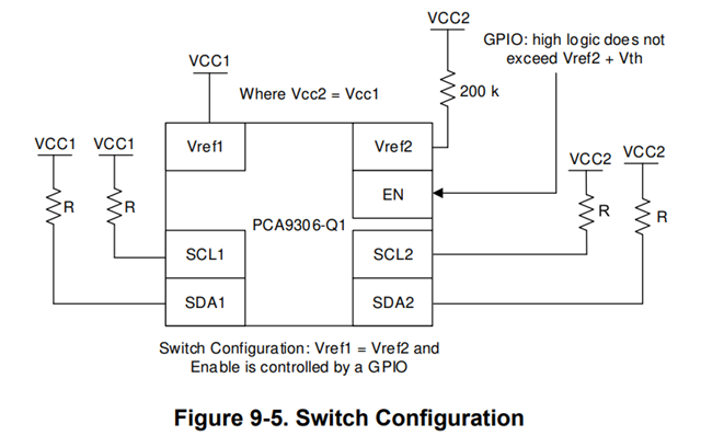
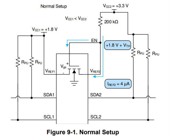
My customer is using PCA9306-Q1 as an I2C switch while VREF1=VREF2=1.8V. I have a question about the voltage selection of EN pin. Why we can't choose high logic to exceed Vref2+Vth? My understanding is that this will help reduce the Rds(on) of internal FET. In such condition(VREF1=VREF2=1.8V), there will not be too much current flowing between VREF1 and VREF2.

What is the purpose of internal FET between VREF1 and VREF2? Is it used for start-up only? There're also extra two FETs between SDA1&SDA2/SCL1&SCL2 right?

BR,

Oliver Tang

  • The gates of all transistors are connected together.

    In the normal setup, the reference transistor, together with the 200 kΩ resistor, ensures that the voltage at the EN pin is above VREF1 by the threshold voltage. This means that the transistors switch off only for voltages above VREF1, which makes transmissions faster because the gate does not have to be completely (dis)charged.

    In the switch configuration, the voltages at VREF1 and VREF2 do not really matter (they do not affect the other transistors; you could use them as a third channel). The EN pin directly determines the gate voltage of all transistors. A higher voltage indeed decreases Rds(on) by a little. The specified limit of Vref2 + Vth prevents the transistor switch from being closed for high-level signals, but this would be necessary only for level shifting. So there is indeed no reason for this limit. (In practice, connecting EN to VCC is often the easiest solution.)

    Also see [FAQ] How do the LSF translators work?