We are using a TI parts in our application. For those parts we have attached schematic file below which we design. Please review schematic and let us know your comments.
Thanks,
Sonali
This thread has been locked.
If you have a related question, please click the "Ask a related question" button in the top right corner. The newly created question will be automatically linked to this question.
We are using a TI parts in our application. For those parts we have attached schematic file below which we design. Please review schematic and let us know your comments.
Thanks,
Sonali
Please find the attached schematic below
Hi Sonali,
So to preface my comments - the THVD1426 in this schematic looks fine, no issues. However - there are some considerations that I want to double check were taken into consideration during the design process.
My comment deals with resistors R134 and R136 - I know they are DNP - but I want to understand the values picked.
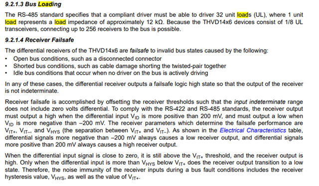
1. Are these resistors used as an external fail-safe (during open/idle/short bus conditions and the device is in RX mode will create a logic high on the "R" pin)?
2. If yes on the above question, how many nodes is this system supporting? Does the system contain 2 termination resistors connected (I see the term in the schematic but there is a switch which implies that you may switch off termination)
3. If placed in the system - how many nodes would have these external resistors?
4. Are all transceivers on the bus the same part (THVD1426) or there other part numbers - if so can I know the max number of nodes they support (this impacts the input resistance of the device which could possibly affect the sizing of R134 and R135)
With all that being said I calculated that if these are fail-safe resistors, in a 2 node system with 2 120 ohm terminations and both transceivers are the THVD1426 to have an idle differential voltage between A and B to be just above 200mV with 620 Ohm resistors (only placed on 1 node - external biasing resistors are best used on 1 node only - the entire bus will be affected by the one node) - which is fine for an external fail safe biasing network. However if there are more than 2 nodes in the system and/or have different transceivers on the bus the input resistance of the other transceivers could start to affect the sizing requirements of those resistors.
So overall the schematic looks good - I just want to double check the sizing on the fail-safe resistors with respect to the entire system - if it is for a low node system where all the devices on the bus can support 256 nodes like the THVD1426 the 620 is probably okay but high node systems or transceivers that can support less than 256 could influence that value.
Please let me know!
Best,
Parker Dodson
Hi Parker,
Thanks for the reply.
The THVD1426 device provides failsafe operation without a need for the external failsafe bias resistors.

Also, other the THVD1426 we have used SN65DSI83ZXHR, TPS7A7001DDAR and TPS3851H18EDRBR parts in our schematic design which we have already shared with you.
Can you please review these parts also?
Thanks,
Sonali
Hi Sonali,
1. External fail-safes are still common with devices with integrated fail-safe to add more noise margin around 0V as typically fail-safe devices are not very noise immune at bus idle conditions and external failsafe's apply to the entire bus not just one device. You don't need them - I brought it up as you do have the pads in the schematic for it and they seem to be properly sized for common applications.
2. I have added the high speed interface team to look at the SN65DSI83ZXHR in the schematic to review; as my experience is in RS-485/RS-422. For increased speed of response I'd also post a question in the power management forum to get a review of the power electronics as they will have the most beneficial advise.
Best,
Parker Dodson
Hi Sonali,
Please see attached for my DSI83 review comment.
SC606 CPU CARD_TI_Reviewed_06152022.pdf
Thanks
David