This thread has been locked.

If you have a related question, please click the "Ask a related question" button in the top right corner. The newly created question will be automatically linked to this question.

TPS65988EVM: TPS65988EVM

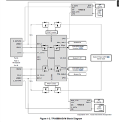
Part Number: TPS65988EVM

Hi,

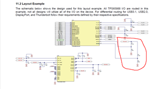
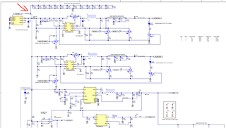
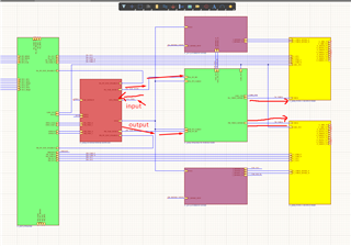
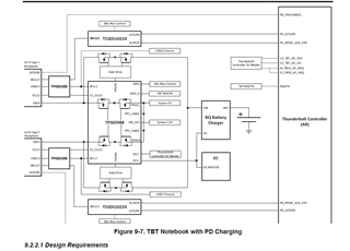
I have some questions regarding a custom PCB by following the reference design of TPS65988EVM.


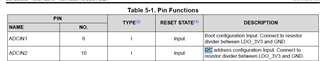
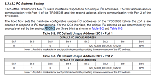
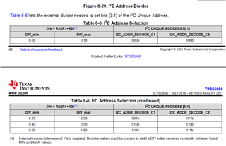
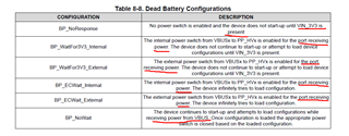
  1. Why do I need multiple I2C addresses? Can't I use one I2C address for a custom board e.g. 191K and 100K voltage divider?
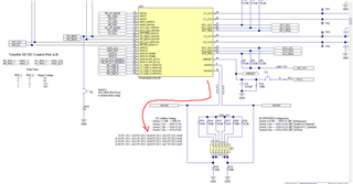
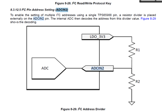
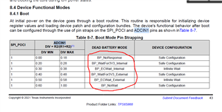
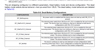
  2. What is the function of the ADCIN1 pin? I don't understand it. I need some explanation and can I add simple a voltage divider for my application instead of multiple?
    Application:
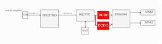
    Want to use TPS65988 as a source for two sink peripherals connected with USB  C ports
  3. I also need help in selecting a buck/boost IC to provide 20V 5A input to TPS65988EVM. I have TPS25750EVM connected with a lipo battery 4S 4.5A. The TPS25750EVM input is connected with a 100W PD wall adapter.
    As I also need approx 80W power from the output of TPS65988EVM. But BQ25792 allows 66W power at SYS pin. So I need to boost or buck input power for TPS65988. 

Any suggestion or guidelines are appreciatable. Thanks

  • Hi Ali,

    I would recommend taking a look at the TPS65988 datasheet and Technical Reference Manual as it will provide more info on the I2C and ADCINx pin descriptions and configurations. Which I2C port are you referring to also? There are 3 different I2C ports on the PD controller for different purposes.

    Thank you,

    Hari

  • Hi 
    I read the datasheet and when I didn't understand, I posted it here otherwise I never do that to waste your time.
    Let me know if you can help me to get the answer to the above questions.
    Thanks

  • I'm looking into it, I'll get back to you shortly

  • Hey Ali,

    1.) For the first question, I may need more information to understand the problem better. My recommendation is to follow the data table on page 28 of the TPS56988 user guild. Below a link to the datasheet.

     TPS65988_datasheet

    2.) I believe the purpose of ADCIN1 is to convert the analog signal of the voltage divider and convert that into digital bits the for the I2C addresses. 

    3.) I'm unsure how to answer this question, as it sounds highly custom.

    Best,

    Erik

  • Hi
    Thanks for your reply.
    1: I am following TPS65988EVM design and I  found there is a dip switch which is connected with ADCIN2 pin along with different resistors values. With different switches configuration, we can setup different I2C addresses. I am curious why we need different I2C addresses. Mostly devices have single I2C address belong to I2C port. Also, do i need different I2C address at any programming part? 


    Now as you can see, we can setup different I2C addresses with different voltage divider configuration. Now my question is what is the purpose of having multiple addresses. Why anyone need to setup different address? What issue  i might face if i setup to a fixed address using single voltage divider?
    I am sure there must be some reason that's why TI introduced this setting.

    Layout Example

    2: I really don't understand about ADCIN1 settings.

  • Hey, Ali

    1. At a high level the PD controller in your figure may be a part of a larger Inter-Integrated Circuit (I2C) network. The network can only work if each device has its own unique address. Consequently, it is important to change the address to meet this I2C requirement.
    2. In this documentation the voltage division of ADC1IN determines the response of the PD controller during a dead battery boot. Each response is detailed in table 8-8. Each response references startup operations given the conditions of VIN_3V3.

    Please let me know if this information was satisfactory.

    Best, 

    Erik

  • Hi,
    In my design, I have only TPS25750, BQ25792 and TPS65988. I will check the other two devices address and if it is different then i will choose a voltage divider to use a some unique single I2C address. I can't add dip switch due to tight space.
    2:
    It is all about Dead battery configuration. Right?
    In my case,  I don't have any battery connected with TPS65988. It will get power directly from DC jack port . Also, I am not using external power path because i have to use TPS65988 as a source for USB C ports.


    The DC jack port is getting constant input power i.e. 20V and 5A.


    In my understanding, It is use to enable or disable different switch of TPS65988 based on the power available at PORTS which is the case if it is use as a sink while I am using TPS as a source for both devices. Correct me if i am wrong.
    Thanks

  • 1. It sounds like you have the right idea. Be sure to do your homework on I2C. Here is a good resource on I2C. 

    2. I believe BP stands for battery power (BP). If there is no battery I would assume that you would want to use the BP_NoResponse configuration. I think there may be some confusion regarding whether this device is sinking or sourcing power. A Source delivers power, if the TPS is receiving power from a barrel jack then your device is behaving as a sink. I'm blind to the full block diagram of your project, but the TPS can behave as a 5V source. Exactly how should be in the documentation. 

    Best,

    Erik

  • Hi
    Thanks again for the link provided. I really appreciate all your help.
    Here is the block diagram of my system that i am trying to develop. I also attached the schematic of my design.
    I think i am at wrong track because someone guided me here that i need to use TPS25750 as a sink because it will take input from wall adapter but when its output will connect with TPS65988 then TPS65988 will act as a source for the sink devices connected attached at USB C ports. Let me know if am wrong.
    Thanks


    POWER DISTRIBUTION BOARD.pdf

  • Hey Ali, 

    On this block diagram it looks as though there is a battery connected so be sure to configure your devices accordingly. I believe you are correct, on this block diagram the TPS65988 is acting like a sink for the labeled source devices. I recommend learning about the EVM's dual role port (DRP) capabilities. Specifically how DRP's would work in this block diagram. Again there is only so much help I can provide for design specific questions. 

    Best,

    Erik

  • Hi 
    If I use TPS65988EVM and connect DC jack port power with it and also connect two power consuming devices with its USB C ports then Isn't it will act as a source?
    Now the DC jack port power can be either battery power or some wall adapter power. I think it doesn't matter. I believe you are considering TPS65988EVM according to this block diagram.

    While I am following this block diagram(eliminated display ports circuits).

    Can you review my schematic plz? I attached in my previous reply.
    Thanks

  • Hi 
    Is there any update or questions regarding my query?

    Plz help me to understand it.
    Thanks

  • Hello Ali, 

    This is much different than the original question. Could you please open this as a new thread.

    Best,

    Erik