This thread has been locked.

If you have a related question, please click the "Ask a related question" button in the top right corner. The newly created question will be automatically linked to this question.

DS90UB935-Q1: Question about DS90UB935-Q1 and DS90UB962-Q1

Part Number: DS90UB935-Q1
Other Parts Discussed in Thread: DS90UB962-Q1,

Hello:

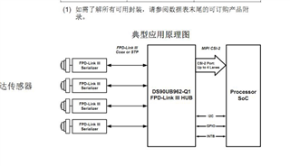
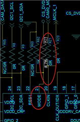
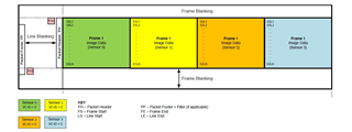
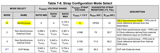
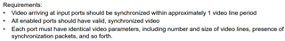
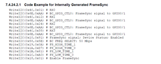
The professional flat panel project has four cameras. The four cameras use TI chips ds90ub935-q1 and ds90ub962-q1

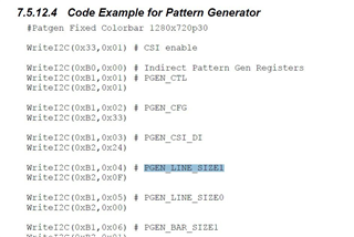
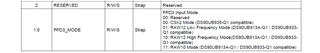
Now the Ti chips need to write registers, and customer wants TI to provide relevant parameter configurations to make the camera work,Please help!!!

  • Hello Jimmy,

    In a system that uses one 962 device and four 935 devices, customer would need to write registers on the TI chips and the connected cameras through I2C register writes. If the processor is connected to the 962's I2C bus, then customer can send I2C writes directly to the 8-bit I2C addresses of the 962 and 935 devices. Customer also needs to make sure that their processor support I2C clock stretching.

    If customer wants to configure the registers in the cameras that are connected to the 935 serializers, then they need to make sure that all of the devices are powered-up and LOCKed first. Then, they need to set the following configurations in the registers in the 962 deserializer device:

    1. Select one of the RX Ports to configure the registers for, by setting the appropriate RX_WRITE_PORT_# bit in register 0x4C
      1. For example, set register 0x4C = 0x01
    2. Enable the I2C_PASS_THROUGH bit in the deserializer.
      1. Set register 0x58[6] = 1
    3. Store the 7-bit I2C address of the camera into bits 7:1 in one of the SlaveID registers (Registers 0x5D - 0x64).
      1. For example, set register 0x5D = 0x## for SlaveID[0]
      2. You can take the 8-bit address and right-shift by one bit to get the 7-bit address.
    4. In the paired SlaveAlias register, store any unique 7-bit I2C address (Registers 0x65 - 6C).
    5. Send an I2C command to the 8-bit SlaveAlias register. The I2C address will get remapped to the paired SlaveID address and can be sued to configure the camera registers.

    Best,

    Justin Phan

  • Hello Justin:

    My client don‘t know how to configure it. Can you provide a reference initialization sequence to the customer in order to make four cameras work normally?Thanks!!!

  • Hello Jimmy,

    Here is an example of how to configure the registers on the 962 to pass I2C commands from the Processor->935->962->Camera. Customer would need to choose the appropriate I2C addresses to fit their application. 

    import time
    
    UB960 = 0x7A # 8-bit I2C address of the 962 device (Set through IDX pin)
    
    #	Port selection, Passthrough, and aliasing
    board.WriteI2C(UB960, 0x4C, 0x01) # Enable read/writes to RX Port 0 registers
    board.WriteI2C(UB960, 0x58, 0x5E) # Set I2C_PASS_THROUGH bit and set Back Channel rate to 50Mbps
    board.WriteI2C(UB960, 0x5D, 0x60) # Store the 7-bit I2C address of the camera in RX Port 0 SlaveID0[7:1]
    board.WriteI2C(UB960, 0x65, 0x18) # Any unique 7-bit I2C address in RX Port 0 SlaveAlias0[7:1]										#953a aliasing
    
    board.WriteI2C(UB960, 0x4C, 0x12) # Enable read/writes to RX Port 1 registers
    board.WriteI2C(UB960, 0x58, 0x5E) # Set I2C_PASS_THROUGH bit and set Back Channel rate to 50Mbps
    board.WriteI2C(UB960, 0x5D, 0x60) # Store the 7-bit I2C address of the camera in RX Port 1 SlaveID0[7:1]
    board.WriteI2C(UB960, 0x65, 0x20) # Any unique 7-bit I2C address in RX Port 1 SlaveAlias0[7:1]												#953b aliasing
    
    board.WriteI2C(UB960, 0x4C, 0x24) # Enable read/writes to RX Port 2 registers
    board.WriteI2C(UB960, 0x58, 0x5E) # Set I2C_PASS_THROUGH bit and set Back Channel rate to 50Mbps
    board.WriteI2C(UB960, 0x5D, 0x60) # Store the 7-bit I2C address of the camera in RX Port 2 SlaveID0[7:1]
    board.WriteI2C(UB960, 0x65, 0x22) # Any unique 7-bit I2C address in RX Port 2 SlaveAlias0[7:1]												#953c aliasing
    
    board.WriteI2C(UB960, 0x4C, 0x38) # Enable read/writes to RX Port 3 registers
    board.WriteI2C(UB960, 0x58, 0x5E) # Set I2C_PASS_THROUGH bit and set Back Channel rate to 50Mbps
    board.WriteI2C(UB960, 0x5D, 0x60) # Store the 7-bit I2C address of the camera in RX Port 3 SlaveID0[7:1]
    board.WriteI2C(UB960, 0x65, 0x24) # Any unique 7-bit I2C address in RX Port 3 SlaveAlias0[7:1]												#953d aliasing
    
    board.WriteI2C(UB960, 0x4C, 0x01) # Enable read/writes to RX Port 0 registers
    # Send I2C commands to the camera connected to RX Port 0 to initialize it (0x18)
    
    board.WriteI2C(UB960, 0x4C, 0x12) # Enable read/writes to RX Port 1 registers
    # Send I2C commands to the camera connected to RX Port 1 to initialize it (0x20)
    
    board.WriteI2C(UB960, 0x4C, 0x24) # Enable read/writes to RX Port 2 registers
    # Send I2C commands to the camera connected to RX Port 2 to initialize it (0x22)
    
    board.WriteI2C(UB960, 0x4C, 0x38) # Enable read/writes to RX Port 3 registers
    # Send I2C commands to the camera connected to RX Port 3 to initialize it (0x24)

    Let me know if there are any questions.

    Best,

    Justin Phan

  • Hi Justin:

    Is this initialization sequence complete? The customer didn't find the relevant control of CSI and didn't know how the data came out.

    At present, the customer wants to adjust the Ti chip separately and set the ti962 chip to pattern mode. The customer refers to the example in the document. At present, I2C is connected, but Mipi has no data output

    As shown in the figure below, the pattern mode of ti962 has been running, but writing registers into 935 through 962 will report an error. The customer does not know how to debug

  • Hello Jimmy,

    Right now, it seems customer can use PATGEN, but they are still having issues communicating with the connected 935 serializer.

    The script I shared is an example of how to configure the I2C_PASS_THROUGH settings on the 962 device and allow the Host to send an I2C command over the FPD-Link devices, from Host->962->935->Camera.

    Customer would have to incorporate that into their script and change several settings to fit their actual use case. But this code is for programming registers in remote slave devices connected to I2C bus of the serializer, such as the cameras. If you just want to program the registers in the connected 935 serializers, then this should be possible if you are able to establish a stable LOCK between the 962 and 935.

    Can you perform the following checks?

    1. Can you make sure that the 935 and 962 are in compatible MODE settings?
    2. Can you verify that the 962 and the 935 have a stable LOCK?
      1. Set register 0x4C to read one of the RX Port registers and then read register 0x4D on the 962 multiple times?
      2. The LOCK_STS_CHG bit should remain 0 after multiple reads and the LOCK_STS bit should remain set to 1.
    3. The SER_ALIAS and SER_ID are automatically loaded onto the 962 deserializer after connection. Can you verify that the correct SER_ID was loaded onto the 962 deserializer in register 0x5B and that a unique SER_ALIAS_ID is set in register 0x5C?
      1. First, select one RX Port to read/write to in register 0x4C and then read registers 0x5B and 0x5C in the 962 device. If you want to write to the connected serializer, send an I2C command to the I2C address stored in register 0x5C.

    Best,

    Justin Phan

  • Hi Justin:

    The following is the current set sequence:

      {0x6d,0x78, 0x10}, \

      {0x4c,0x01, 0x10}, \

      {0x58,0x5e, 0x10}, \

      {0x5c,0x19, 0x10}, \

      {0x5d,0x19, 0x10}, \

      {0x65,0x19, 0x10}, \

    The following is some register information read after writing the above sequence.

    [   35.426530] ti_sensor_reg_read reg 0x3  value 0x40

    [   35.430947] ti_sensor_reg_read reg 0x6d  value 0x78

    [   35.435534] ti_sensor_reg_read reg 0x4d  value 0x30

    [   35.440225] ti_sensor_reg_read reg 0x5b  value 0x32

    [   35.445298] ti_sensor_reg_read reg 0x4d  value 0x0

    [   35.450026] ti_sensor_reg_read reg 0x4d  value 0x0

    [   35.454898] ti_sensor_reg_read reg 0x4d  value 0x0

    [   35.459591] ti_sensor_reg_read reg 0x4d  value 0x0

    [   35.464424] ti_sensor_reg_read reg 0x0  value 0x64

    1、Can you make sure that the 935 and 962 are in compatible MODE settings?

    The customer reads 0x6d as 0x78 through ti962 and confirms that it is compatible mode

    2、Can you verify that the 962 and the 935 have a stable LOCK?

    After reading 0x4d, it is found that: lock_ STS bit is not set to 1, which indicates that there is no lock. Customer doesn‘t know what is the reason.

    The customer currently has a problem with the camera connector and cannot debug it. He wants to set the two chips to the pattern mode. The pattern generated by ti962 has been plotted. Now he needs to debug the relevant channels of ti935. Please tell me how to configure the register, write the register to ti935, and control 935 to generate a pattern. Thank you!!!

  • Hello Jimmy,

    The first step you should focus on is making sure the 962 and 935 are able to LOCK onto each other. There are multiple reasons why LOCK is not set on the 962. Can you go through the following checklist?

    1. Can you provide the schematic for the 962?
      1. I want to double-check to make sure there are no issues in the schematic.
      2. This is a public forum, so if you do not feel comfortable posting it here, you can message me privately.
    2. What is the MODE setting on the 935?
      1. Are able to provide the schematic for the 935 as well?
    3. Is your 935 and 962 connected over a COAX cable?
      1. If so, could you try the steps listed below in (4)?
    4. In the 962 device, can you try setting register 0x6D = 0x7C?
      1. First, select one of the RX Ports on the 962 by configuring register 0x4C. If the 935 is connected to RX Port 0, then set register 0x4C = 0x01.
      2. Next, set register 0x6D = 0x7C.
      3. Finally, read register 0x4D multiple times to see if you can get it to read 0x03.
    5. Can you double-check and make sure that the 962 device is powered-up correctly, by probing the power supply pins on the 962 and verifying that the Power-Up Sequence defined in the 962 datasheet was strictly followed?
      1. Post the oscilloscope screenshots.
    6. Can you double-check and make sure that the connected 935 device is powered-up properly, by probing the power supply pins on the 962 and verifying that the Power-Up Sequence defined in the 935 datasheet was strictly followed?
      1. Post the oscilloscope screenshots.
    7. Are you able to power the 935 device locally and access the I2C bus on the 935 device directly?
      1. You can use some type of processor on the local 935 I2C bus or use a tool like USB2ANY to connect a lab computer to the 935 I2C bus and then communicate with the 935 device through ALP.

    Best,

    Justin Phan

  • Hi Justin:

    1、Can you provide the schematic for the 962?——schematic diagram

    2、What is the MODE setting on the 935?——schematic diagram

    3、Is your 935 and 962 connected over a COAX cable?——Not connected by coaxial line

    4、In the 962 device, can you try setting register 0x6D = 0x7C?——Not connected by coaxial line

    5、Can you double-check and make sure that the 962 device is powered-up correctly, by probing the power supply pins on the 962 and verifying that the Power-Up Sequence defined in the 962 datasheet was strictly followed?——External long power supply

    6、Can you double-check and make sure that the connected 935 device is powered-up properly, by probing the power supply pins on the 962 and verifying that the Power-Up Sequence defined in the 935 datasheet was strictly followed?——External long power supply

    7、Are you able to power the 935 device locally and access the I2C bus on the 935 device directly?——No relevant tools

    RSK_R366_CAM_V1.0_20220117.pcb

    RSK_R366_CAM_V1.0_20220117.sch

  • Hello Jimmy,

    Let me take a look at the schematics and return with comments.

    For the 935 board, can you confirm that it is powered-up correctly by replicating the Power-Up Sequence on an oscilloscope?

    Is there any other system that you can connect to the 935 PCB, in order to confirm that the 935 is powered-up and is capable of sending video data from an imager? Or do you have a setup where you can power the 935 separately and then confirm it is possible to communicate to the 935 device through I2C?

    It sounds like you can configure the 962 properly. If you can confirm the 935 is powered-up correctly as well and that it is possible to read/write registers in the 935 device through I2C, then the only reason why LOCK is not HIGH is because there is an issue with the Return Loss/Insertion Loss/Impedance between the FPD-Link channel.

    We can continue in this debug direction if you can confirm the 935 is functioning correctly.

    Best,

    Justin Phan

  • Hi Justin:

    Here, connect the I2C of 935 to the host for reading and writing, and it can communicate normally. The following is the information read out by 935


    [   35.236378] ti962_sensor_reg_read reg 0x3  value 0x40

    [   35.239823] ti962_sensor_reg_read reg 0x6d  value 0x78

    [   35.244881] ti962_sensor_reg_read reg 0x4d  value 0x30

    [   35.249818] ti962_sensor_reg_read reg 0x5b  value 0x32

    [   35.255014] ti962_sensor_reg_read reg 0x4d  value 0x0

    [   35.260070] ti962_sensor_reg_read reg 0x4d  value 0x0

    [   35.265284] ti962_sensor_reg_read reg 0x4d  value 0x0

    [   35.270172] ti962_sensor_reg_read reg 0x4d  value 0x0

    [   35.275281] ti962_sensor_reg_read reg 0x0  value 0x64

    [   35.279807] msm_sensor_config32:CFG_SLAVE_WRITE_I2C_ARRAY:

    [   35.284894] msm_sensor_config32:slave_addr=0x32, array_size=31 addr_type=1 data_type=1

    [   35.290238] msm_sensor_config32:orig_slave_addr=0x32, new_slave_addr=0x19

    [   35.308644] ti935_sensor_reg_read reg 0x0  value 0x32

    [   35.309113] ti935_sensor_reg_read reg 0x2  value 0x33

    [   35.313274] ti935_sensor_reg_read reg 0x6  value 0x41

  • Hello Jimmy,

    1. You mentioned previously that in the 962, register 0x6D = 0x78, which means the 962 is in CSI-2 Mode. This will be Synchronous Mode (50Mbps) by default.
      1. Could you clarify what is the MODE on the connected 935, by looking at the MODE strap settings on the 935 PCB or by reading register 0x03 on the 935?
    2. If the 935 and 962 are powered-up correctly and set to the matching MODES, then the devices should be able to LOCK at power-up.
      1. Can you try not running the initialization script and just power-up the connected 935/962 devices, and then see if LOCK is established by reading register 0x4D several times?
    3. I also couldn't open the schematic file that you shared with me, so could you share the schematic in a PDF?

    Best,

    Justin Phan

  • Hello Justin:

    The PDF schematic diagram is attached. The pull-up resistance on the mode pin is removed. Now it can be locked, but it still cannot communicate through 962 and 935, and an error is reported when reading and writing registers.Why can't I write CMD into 935 through 962?

    Here is the print information:

     01-13 02:18:42.908     0     0 E         : ti962_sensor_reg_read reg 0x3  value 0x40

    01-13 02:18:42.908     0     0 E         : ti962_sensor_reg_read reg 0x6d  value 0x78

    01-13 02:18:42.912     0     0 E         : ti962_sensor_reg_read reg 0x4d  value 0x13

    01-13 02:18:42.917     0     0 E         : ti962_sensor_reg_read reg 0x5b  value 0x32

    01-13 02:18:42.922     0     0 E         : ti962_sensor_reg_read reg 0x4d  value 0x3

    01-13 02:18:42.933     0     0 I chatty  : uid=0(root) logd identical 2 lines

    01-13 02:18:42.938     0     0 E         : ti962_sensor_reg_read reg 0x4d  value 0x3

    01-13 02:18:42.942     0     0 E msm_sensor_config32: CFG_SLAVE_WRITE_I2C_ARRAY:

    01-13 02:18:42.947     0     0 E msm_sensor_config32: slave_addr=0x32, array_size=31 addr_type=1 data_type=1

    01-13 02:18:42.953     0     0 E msm_sensor_config32: orig_slave_addr=0x32, new_slave_addr=0x19

    01-13 02:18:42.961     0     0 E msm_cci_irq: 1807 MASTER_0 error 0x8000000

    01-13 02:18:43.057     0     0 E msm_cci_wait: 306 wait for queue: 0

    01-13 02:18:43.057     0     0 E msm_cci_transfer_end: 568 failed rc -110

    01-13 02:18:43.061     0     0 E msm_cci_data_queue: 816 failed rc -110

    01-13 02:18:43.066     0     0 E msm_camera_cci_i2c_write_table_cmd: line 216 rc = -110

    01-13 02:18:43.071     0     0 E msm_cci_i2c_read: 965 read_words = 0, exp words = 1

    01-13 02:18:43.077     0     0 E msm_cci_irq: 1807 MASTER_0 error 0x10000000

    01-13 02:18:43.082     0     0 E msm_cci_i2c_read_bytes: 1048 failed rc -22

    01-13 02:18:43.088     0     0 E msm_camera_cci_i2c_read: line 47 rc = -22

    01-13 02:18:43.093     0     0 E         : ti935_sensor_reg_read reg 0x0  value 0x0

    01-13 02:18:43.098     0     0 E msm_cci_i2c_read: 965 read_words = 0, exp words = 1

    01-13 02:18:43.103     0     0 E msm_cci_irq: 1807 MASTER_0 error 0x10000000

    01-13 02:18:43.108     0     0 E msm_cci_i2c_read_bytes: 1048 failed rc -22

    01-13 02:18:43.113     0     0 E msm_camera_cci_i2c_read: line 47 rc = -22

    01-13 02:18:43.119     0     0 E         : ti935_sensor_reg_read reg 0x2  value 0x0

    01-13 02:18:43.124     0     0 E msm_cci_i2c_read: 965 read_words = 0, exp words = 1

    01-13 02:18:43.129     0     0 E msm_cci_irq: 1807 MASTER_0 error 0x10000000

    01-13 02:18:43.134     0     0 E msm_cci_i2c_read_bytes: 1048 failed rc -22

    01-13 02:18:43.140     0     0 E msm_camera_cci_i2c_read: line 47 rc = -22

    01-13 02:18:43.145     0     0 E         : ti935_sensor_reg_read reg 0x3  value 0x0

    01-13 02:18:43.150     0     0 E msm_cci_i2c_read: 965 read_words = 0, exp words = 1

    01-13 02:18:43.155     0     0 E msm_cci_irq: 1807 MASTER_0 error 0x10000000

    01-13 02:18:43.160     0     0 E msm_cci_i2c_read_bytes: 1048 failed rc -22

    01-13 02:18:43.165     0     0 E msm_camera_cci_i2c_read: line 47 rc = -22

    01-13 02:18:43.171     0     0 E         : ti935_sensor_reg_read reg 0x6  value 0x0

    RSK_R366_CAM_V1.0_20220117.pdf

  • Hello Jimmy,

    The team is currently OoO due to the US holiday and will return to office on 7/5. Thank you for your patience during this time 

    Best Regards,

    Casey

  • Hello Jimmy,

    I still can't open the schematic on my computer. Is there any way you can fix the PDF or provide another format?

    Also, if you removed the pull-up resistor on the MODE pin of the 935, then it seems like you originally had it in Non-Synchronous MODE or some other MODE. By removing the pull-up resistor on the 935 MODE pin, you will likely set it to Synchronous MODE. This will match the MODE on the 962 and get it to LOCK. 

    1) Can you confirm which operating MODE the designer wishes for the connected 935/962 to operate in?

    2) In a previous post, you mentioned that on the 962, register 0x5B = 0x32 and register 0x5C = 0x19. After the 935 and 962 LOCK, the I2C address of the connected serializer will automatically load onto the deserializer in register 0x5B.

    a) Can you confirm that 0x32 is the correct I2C address of the connected 935 serializer?

    b) Since you set register 0x5C = 0x19, you are actually setting the SER_ALIAS_ID to 0x18, since the last bit in that register sets the AUTO_ACK bit. Can you try sending an I2C command to the I2C address of 0x18 and see if it works?

    Best,

    Justin Phan

  • Hello Justin:

    Attached are schematic diagrams, PDF drawings

    3240.RSK_R366_CAM_V1.0_20220117.pdf

    935 mode pin has a pull-up of 4.7K and a pull-down resistance. Should the pull-down resistance be removed?? Are the four ICs synchronized?

    At present, we require four cameras to work at the same time to display four images, and one is displayed on the screen

    Now customers can lock, I2C can also communicate normally, and a single ti962->ti935->camera can plot normally. However, we need to synthesize four cameras in the following way. Please provide the configuration method of registers: Thanks!!!

  • The following is the current set sequence,  Unable to plot, help check it.   a single ti962->ti935->camera can plot normally.

    4353.reg.txt
    # DS90UB936-Q1 Settings  
      {0x4c,0x01, 0x0}, \
      {0x58,0x5e, 0x0}, \
      {0x5c,0x32, 0x0}, \
      {0x5d,0x32, 0x0}, \
      {0x65,0x18, 0x0}, \
      {0x70,0x2b, 0x0}, \
      {0x4c,0x12, 0x0}, \
      {0x58,0x5e, 0x0}, \
      {0x5c,0x32, 0x0}, \
      {0x5d,0x32, 0x0}, \
      {0x65,0x20, 0x0}, \
      {0x70,0x2b, 0x0}, \
      {0x4c,0x24, 0x0}, \
      {0x58,0x5e, 0x0}, \
      {0x5c,0x32, 0x0}, \
      {0x5d,0x32, 0x0}, \
      {0x65,0x22, 0x0}, \
      {0x70,0x2b, 0x0}, \
      {0x4c,0x38, 0x0}, \
      {0x58,0x5e, 0x0}, \
      {0x5c,0x32, 0x0}, \
      {0x5d,0x32, 0x0}, \
      {0x65,0x24, 0x0}, \
      {0x70,0x2b, 0x0}, \
      
      {0x4c,0x01, 0x0}, \
    # DS90UB935-Q1 Settings pattern test
      {0x4c,0x12, 0x0}, \
    # DS90UB935-Q1 Settings pattern test
      {0x4c,0x21, 0x0}, \
    # DS90UB935-Q1 Settings pattern test
      {0x4c,0x38, 0x0}, \
    # DS90UB935-Q1 Settings pattern test
    
      {0x32,0x01, 0x0}, \
      {0x33,0x01, 0x0}, \
      {0x21,0x3c, 0x0}, \
      {0x20,0x00, 0x0}, \
    

  • Hello Jimmy,

    1) Since the 962 seems to be strapped to "CSI-2" Mode, then the 962 is in CSI-2 Synchronous Mode by default. In the 935, you want to match the Mode set on the deserializer. To do this, remove the pull-up resistor and keep the pull-down resistor.

    Please see the Strap Configuration Mode Select tables in each device datasheet for more details. 

    For now, both the 935 and 962 are set to CSI-2 Synchronous Mode, which will allow the devices to communicate with each other and send video.

    2) The image you are showing is for a type of synchronized forwarding method that the 962 implements on received video data called Line-Concatenated CSI-2 Forwarding. The 962 datasheet has an example of how to configure the 962, but needs to be modified, since your 935/962 are operating in CSI-2 MODE. 

    # "*** RX0 VC=0 ***"
    WriteI2C(0x4C,0x01) # RX0
    WriteI2C(0x72,0x00) # RX0 Map all VC-ID to VC0
    # "*** RX1 VC=0 ***"
    WriteI2C(0x4C,0x12) # RX1
    WriteI2C(0x72,0x00) # RX1 Map all VC-ID to VC0
    # "*** RX2 VC=0 ***"
    WriteI2C(0x4C,0x24) # RX2
    WriteI2C(0x72,0x00) # RX2 Map all VC-ID to VC0
    # "*** RX3 VC=0 ***"
    WriteI2C(0x4C,0x38) # RX3
    WriteI2C(0x72,0x00) # RX3 Map all VC-ID to VC0
    # "CSI_PORT_SEL"
    WriteI2C(0x32,0x01) # CSI0 select
    # "CSI_EN"
    WriteI2C(0x33,0x01) # CSI_EN & CSI0 4L
    # "*** CSI0_SYNC_FWD synchronous forwarding with line concatenation ***"
    WriteI2C(0x21,0x0C) # synchronous forwarding with line concatenation
    # "***FWD_PORT all RX to CSI0"
    WriteI2C(0x20,0x00) # forwarding of all RX to CSI0

    Can you integrate the above register writes in your script and see if it works? I saw that the script attached by Gao does register writes to register 0x70 in the 962, but that is not needed since you are not operating in RAW10 Mode. 

    3) If the initialization script still does not work after updating the register writes, can you read register 0x22 in the 962 and post it?

    Best,

    Justin Phan

  • After the update register is written, the initialization script still does not work. The Soc  have csid  and csiphy error.   The following is the information read out

    [ 122.131619] ti962_sensor_reg_read reg 0x22 value 0x0

  • Hello Gao,

    1. Could you post the updated initialization script, so that I can review in more detail?
    2. Are you using the internal or external FrameSync functionality of the 962 device?
      1. For all of the Synchronized Forwarding Modes, each line of video that is being sent from the connected cameras must arrive at the same time, or within approximately 1 video line period. The connected cameras must also send video with the same video timing parameters.
      2. In order to make sure that each camera is sending video at the same time to the 962 DES, you would normally send a FrameSync signal to each connected serializer, which would be outputted on one of the GPIO pins on the serializer and then fed into the FrameSync pin on the camera module.
    3. Can you verify that the following conditions are met in your system?
      1. If the following conditions are not met, then register 0x22 = 0x00. Also, check register 0x35, since the TX_PORT_SYNC register bit should be set to 1 if the input video streams are being sent in a synchronized manner.
    4. Are you also able to create a separate test script that forwards data in Round-Robin Mode, just to make sure that data can be outputted at the CSI-2 TX Port on the 962 with no issues?

    Best,

    Justin Phan

  • The following is the current set sequence.   The framsync pin  have no  connect to camera module in schematic .  Can you help me review the schematic diagram? Is there any other problem?

    2620.reg.txt
    # DS90UB962-Q1 Settings  
      {0x4c,0x01, 0x0}, \
      {0x58,0x5e, 0x0}, \
      {0x5d,0x60, 0x0}, \
      {0x65,0x18, 0x0}, \
      {0x72,0x00, 0x0}, \
      {0x4c,0x12, 0x0}, \
      {0x58,0x5e, 0x0}, \
      {0x5d,0x60, 0x0}, \
      {0x65,0x20, 0x0}, \
      {0x72,0x00, 0x0}, \
      {0x4c,0x24, 0x0}, \
      {0x58,0x5e, 0x0}, \
      {0x5d,0x60, 0x0}, \
      {0x65,0x22, 0x0}, \
      {0x72,0x00, 0x0}, \
      {0x4c,0x38, 0x0}, \
      {0x58,0x5e, 0x0}, \
      {0x5d,0x60, 0x0}, \
      {0x65,0x24, 0x0}, \
      {0x72,0x00, 0x0}, \
      
      {0x4c,0x01, 0x0}, \
    #camera settings
      {0x4c,0x12, 0x0}, \
    #camera settings
      {0x4c,0x21, 0x0}, \
    #camera settings
      {0x4c,0x38, 0x0}, \
    #camera settings
    
      {0x32,0x01, 0x0}, \
      {0x33,0x01, 0x0}, \
      {0x21,0x0c, 0x0}, \
      {0x20,0x00, 0x0}, \
    

  • Hello Gao,

    You cannot use any Synchronized Forwarding on the 962 device, such as the Line-Concatenated CSI-2 Forwarding, unless the video data sent by each camera arrives at each active RX Port at the same time, or within a skew of 1 video line period.

    The FPD-Link devices can transfer a FrameSync signal from the Deserializer to each of the connected Serializers, through a GPIO pin on the serializer, and cause the cameras to send video at the same time. This will cause each video line to arrive at the RX Ports within roughly the same time and allows the 962 to forward the data in a Synchronized manner.

    If you are not using the FrameSync functionality of our FPD-Link devices, then are you capable of synchronizing the output of each camera through some other external method?

    You can check the skew of the incoming video data by programming the GPIO pins on the 962 to output the received Line Valid (LV) and Frame Valid (FV) signals that it receives from each RX Port and see if they line-up on an oscilloscope.

    If you need to use Line-Concatenated CSI-2 Forwarding, then you need to find some way to synchronize the cameras and have them all send video data to the 962 deserializer at roughly the same time, with minimal skew. If you do not have a connection to the FrameSync pin on the camera module, then you may need to redesign the board.

    If you are okay with using Best Effort Round-Robin Forwarding, then you do not need to worry about what time the video arrives at the 962 deserializer's RX Port. But the data will be aggregated and outputted in a different format, as described in Section 7.4.25.1 Best-Effort Round Robin CSI-2 Forwarding in the 962 datasheet.

    Best,

    Justin Phan

  • Hello Justin:

    We need to synchronize the frames of four cameras. Is it in ti962 or ti935?

    For your former question: Can you confirm which operating MODE the designer wishes for the connected 935/962 to operate in?-

    ----------How do we confirm this mode? What are the differences between these modes? We need four camera data to be synthesized into super frames for the host. Which mode should we use?Thanks!!!

  • Hello Jimmy,

    1. Since you want to use Line-Concatenated CSI-2 Forwarding on the 962, which is a synchronized forwarding method, then all of the cameras that you are using in your system need to be the same resolution, frame rate, etc... The cameras must also send video data to the 962 at the same time. This allows the 962 to take one line of video data that it receives from each camera and then combine that data into the format that you posted, before outputting it at the CSI-2 TX Port.
      1. The most common way to guarantee that each camera is sending video at the same time is to use either the Internal FrameSync or External FrameSync feature of the 962. You can program the 962 to send the same pulse to each of its connected serializers, which will be outputted on one of the GPIO pins on the connected serializer. The designer would then need to connect that GPIO pin to the FrameSync pin on the camera module. The pulse will trigger the camera module to capture a frame of video data. Since each camera module receives the same pulse, each camera will capture video data at the same time and send video to the deserializer at the same time, which allows you to use synchronized forwarding. You would need to check the camera module's datasheet, in order to determine the exact pin and the duration of the pulse.
      2. If video data cannot arrive at the same time at the 962, then video data will be discarded.
      3. You either need to make sure the video data arrives at the same time on the 962 or use an unsynchronized forwarding method instead, such as Round-Robin.
    2. The different MODE settings on the FPD-Link devices configure Forward Channel and Back Channel data rates between the serializer and deserializer devices. If the connected devices have matching MODE settings, then the devices can LOCK and transfer data in either direction. Any MODE can be used. The only difference between each MODE is which reference clock is used to drive the channel and how much video bandwidth is allowed. Since your 962/935 devices can LOCK, then there is no issue with the MODE settings.
      1. Your main issue in this E2E post is not the MODE setting. It is getting the connected camera modules to either send video data at the same time or use a different forwarding mode on the 962.

    Best,

    Justin Phan

  • we need use the Internal FrameSync.   But  we can't measure the waveform from 935 gpio0 by using the following code

  • We found that two cameras 962 can output Mipi data, but three cameras have no Mipi data. Is there a limit on bandwidth? The size of a single camera is 1752*2336

  • Hello Gao,

    After running the example code, you should be able to probe GPIO0 on the 962 device and read the generated FrameSync signal. On the 935, you need to configure the GPIO0 pin to be an output pin by setting register 0x0E = 0x1E, before you probe it.

    For your second question, could you clarify?

    Do you mean that you tried using Line-Concatenated CSI-2 Forwarding with only 2 cameras attached to the 962 and the 962 did output video data, but you failed when 3 cameras were attached?

    If so, you should check register 0x22 in every working and failing scenario. It is possible that you are accidentally meeting the requirements for synchronized forwarding when only 2 cameras are connected. In which case, register 0x22 = 0x01. But it is hard to ensure that all cameras will be synchronized if you do not send a FrameSync signal.

    Or are you talking about the video bandwidth limits of our SER/DES devices?

    The 935/962 supports up to 2.528Gbps of video throughput per camera used. 

    Video Throughput = HActive x VActive x (Frame Rate) x Bits-Per-Pixel x Overhead (Assume 25% if unknown)

    If video bandwidth limits are a concern, could you provide more details on the camera video timing?

    Best,

    Justin Phan

  • We need 30Hz frame synchronization signal, which is only 28.7hz now. The following is the register configuration

    {0x4c,0x01, 0x0}, \
    {0x6e,0xaa, 0x0}, \
    {0x4c,0x12, 0x0}, \
    {0x6e,0xaa, 0x0}, \
    {0x4c,0x24, 0x0}, \
    {0x6e,0xaa, 0x0}, \
    {0x4c,0x38, 0x0}, \
    {0x6e,0xaa, 0x0}, \
    {0x10,0x91, 0x0}, \
    {0x58,0x5e, 0x0}, \
    {0x19,0x15, 0x0}, \
    {0x1a,0xb4, 0x0}, \
    {0x1b,0xc3, 0x0}, \
    {0x1c,0x50, 0x0}, \
    {0x18,0x01, 0x0}, \

  • Hello Gao,

    I tried your register settings on a 962 EVM and was able to output a 30Hz FrameSync signal from GPIO0 on the 962 EVM board.

    DES = 0x60
    SER = 0x18
    
    # Init config
    board.WriteI2C(DES, 0x4C, 0x01)  # RX0
    board.WriteI2C(DES, 0x6E, 0xAA) 
    board.WriteI2C(DES, 0x4C, 0x12)  # RX1
    board.WriteI2C(DES, 0x6E, 0xAA) 
    board.WriteI2C(DES, 0x4C, 0x24)  # RX2
    board.WriteI2C(DES, 0x6E, 0xAA) 
    board.WriteI2C(DES, 0x4C, 0x38)  # RX3
    board.WriteI2C(DES, 0x6E, 0xAA) 
    
    board.WriteI2C(DES, 0x10, 0x91)  # FrameSync status
    board.WriteI2C(DES, 0x58, 0x5E)
    board.WriteI2C(DES, 0x19, 0x15)  # FrameSync HIGH[15:0] = 0x15B4 
    board.WriteI2C(DES, 0x1A, 0xB4)
    board.WriteI2C(DES, 0x1B, 0xC3)  # FrameSync LOW[15:0] = 0xC350
    board.WriteI2C(DES, 0x1C, 0x50)
    board.WriteI2C(DES, 0x18, 0x01)  # Enable FramSync
    
    # By default, the RX Port 0 BC rate is selected, 50Mbps BC = 600ns
    # Period of FrameSync = (1 sec / 30Hz) / 600ns = 55,556 counts
    # FS_HIGH_TIME = 0x15B4 = 5,556
    # FS_LOW_TIME = 50,000
    # 10% Duty Cycle

    In the code that you ran, are you certain that RX Port 0 is configured for Synchronous Mode?

    If so, then are you certain that the oscillator used on the REFCLK pin of the 962 device meets the datasheet specifications, as specified in Table 7-3 in the 962 datasheet?

    The internal FrameSync signal generated by the 962 device is directly related to the reference clock used. If the REFCLK oscillator deviates, then the internal FrameSync signal will deviate.

    Best,

    Justin Phan

  • The problem has been solved.  Thank you for your support. 

  • You are welcome. If there are no other open issues, then I will close this thread. But feel free to post again if you have any questions.