This thread has been locked.
If you have a related question, please click the "Ask a related question" button in the top right corner. The newly created question will be automatically linked to this question.
Hello
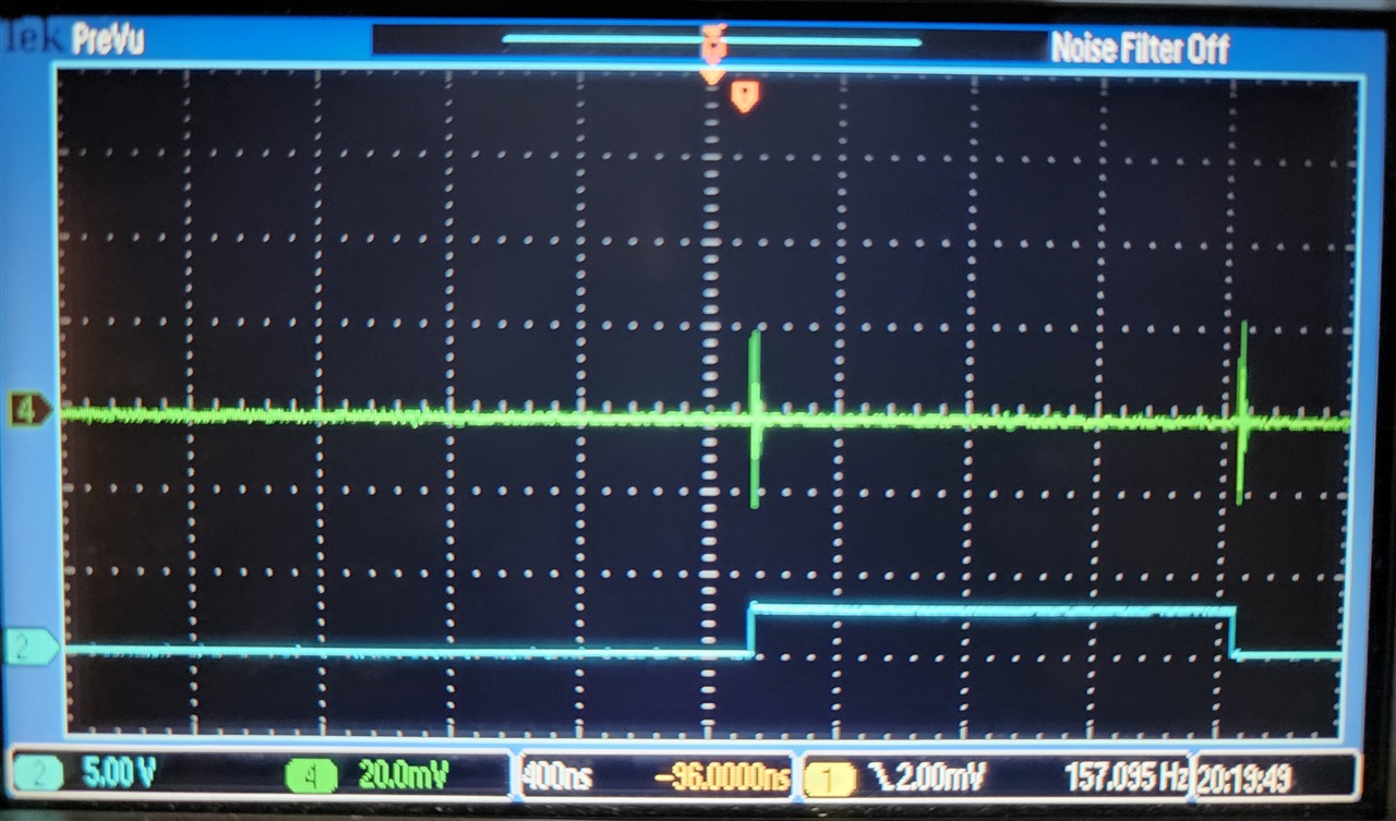
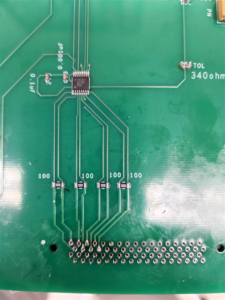
I am seeing undesirable spikes on channels which are suppose to be LOW. The spikes are occuring at the instance when any other channel makes a transition. Please help. Here is a picture of this.
Thank you
Best
Faisal
Hi, Faisal
Can you please share your setup, schematic, and layout?
Thanks
David
Hello David
Here is a snap of the circuit. I am driving TMUX6112 with the output of DSLVDS1048. DSLVDS1048 is taking input from an FPGA board. The complementary inputs are only terminated by 100ohm resistors between them.
Thank you
Faisal
Hi,
Are you seeing the spike only on Rin2+/2 and Rin3+/-?
The 100ohm termination needs to be placed as close to the RX as possible to minimize the signal reflection.
Thanks
David
Faisal
Do you see spike on Rin1+/- if you only toggle Rin4+/-?
Can you also share the schematic and layout of your design?
Thanks
David
David
Yes, and I see spike on the toggled channels as well.
I am using cadence allegro amd orcad. Unfortunately the license got expired so I can't access the schematic now.
Thank you
Faisal
Faisal
The LVDS Standard (ANSI/TIA/EIA-644) specifies a maximum threshold of ±100 mV for the LVDS receiver. I see from the scope capture that you are driving a ~3V signal. Can you lower the signal amplitude on Rin4+/- and see if the spike on Rin1+/- goes away? I am trying to see if the crosstalk among the channels is the root cause here.
Thanks
David
David
The 3V signal is actually a correspondent of the +-100mV LVDS signal coming out of the FPGA. I used this signal to visualize the state transition of the input signals to the receiver.
Please let me know if you find any influence of crosstalk here.
Thanks
Faisal
Faisal
So where does this 3V coming from? I am seeing the noise spike corresponds to the rising and falling of the 3V signal and try to understand the source of this 3V signal.
Thanks
David
David
The 3V or TTL signal is coming from the FPGA unit. The FPGA can give out same signal in multiple forms such as LVDS and TTL. I am applying the TTL signal to the scope to visualize it in scope but driving the receiver IC with +-100mV LVDS signal.
Yes, the spikes are occurring at logic level transitions.
Thanks
Faisal
Faisal
I have the DSLVDS1048 EVM in the lab, please give me a day and let me see if I can duplicate the issue on the EVM.
Any chance of getting the license issue resolved so you can send me the schematic and layout file?
Thanks
David
David
I sincerely thank you for your efforts. Please let me know what you see.
I am expecting to get a renewed license on this thursday.
Best
Faisal
Faisal
I think I am able to reproduce this issue on the EVM and now am looking for a way to reduce the spike. I will update it if I can find a solution.
Thanks
David
Faisal
When you are driving DSLVDS1048 LVDS input, are you driving it differential or single-end? If you are driving differentially, can you reduce the intra-pair skew and see if the spike gets smaller?
Thanks
David
David
I am driving it differentially. In my new design, I will reduce the intra-pair and inter-pair skew. Did you see any other issues while reproducing the scenario? Is crosstalk causing the problem?
Please let me know.
Thank you
Faisal
Faisal
The issue I see on the EVM is not a crosstalk issue. It looks like the intra-pair skew on the input creates a common voltage VCM_skew or common mode noise. This common mode noise gets coupled into the DSLVDS1048 power supply and then affects all the input, resulting in the spike you are seeing in your scope capture.
Thanks
David
Hello David
Thank you so much for the suggestion. I am applying your suggested technique to my new design. Hope it will work.
Best
Faisal