This thread has been locked.

If you have a related question, please click the "Ask a related question" button in the top right corner. The newly created question will be automatically linked to this question.

SN65HVD230: SN65HVD230DR

Part Number: SN65HVD230
Other Parts Discussed in Thread: ISO1050, SN74LV32A, SN65HVD1050, TIDA-01487

Hello,

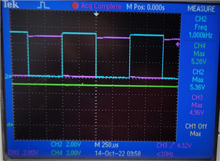
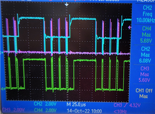
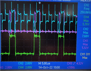
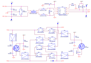
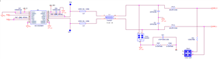
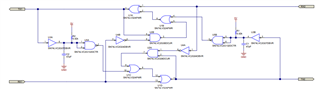
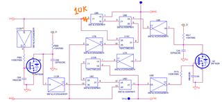
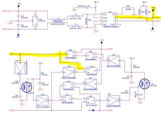
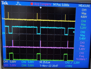
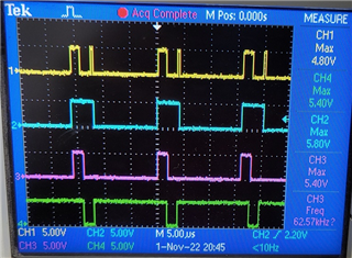
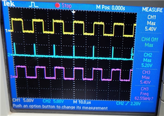
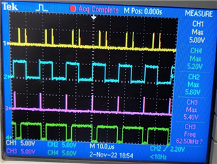
We are using SN65HVD230DR, CAN Transceiver as below

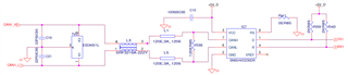
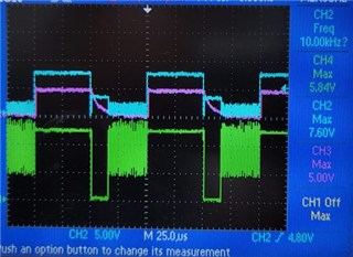
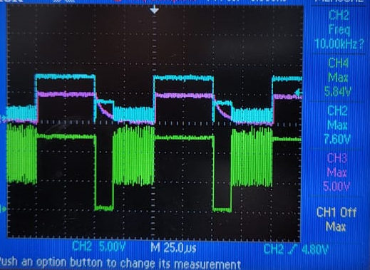
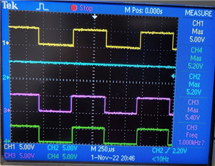
The CAN H and CAN L differential input get distorted as frequency goes above 2kHz. 

As per specification it should support 1MHz.

What should be problem?

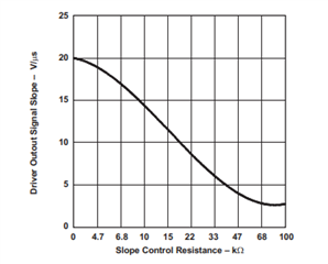
Pin 8 (S) is connected to ground with zero Ohm, I have try with 10K with also but  not improve.

Please Look into this.

What should be the problem?

  • What kind of distortion? Can you show an oscilloscope trace?

  • Hello Clemens,

    Please find below waveforms,

    Ch2:  differential CANH wrt CANL 

    Ch3: RX (Pin4)

    Ch4: Tx (Pin1)

    Waveform taken at 1khz, 10khz and 250khz.

  • at 10kHz,

    at 250kHz,

    Why this happen?

  • Please measure CANH and CANL separately, and check that the oscilloscope inputs are not AC coupled.

    Is there some other device on the bus transmitting?

  • Hi Mayank,

    First, I agree with Clemens please measure the CANH and CANL signals separately. If you only have 3 probes you can leave out the RX signal and keep the TX signal. The other things Clemens asked would be good to know as well.

    Second, I would recommend removing the inductors (L1 and L5). These inductors are not necessary on the bus since you already have a CMC and a CMC is far better at  suppressing common mode noise. The additional inductors here are most likely causing this large overshoot and undershoot. This coupled with the slope control being shorted to GND you have very fast switching voltages. I would also recommend changing the slope control resistor here to slow down your transition especially since you are communicating at such a slow speed. This will help with emissions when you remove those inductors.:

    How many devices do you have on the bus and how many of those devices are terminated with 120 ohms? There should only be two 120 ohm resistors on the entire bus that add in parallel to 60 ohms.

    Best,

    Chris

  • Dear Chris,

    The application is about CAN to CAN Isolation.

    The middle circuit is of Bus Arbitration logic.

    Today I have tested the SN65HVD1050MDREP IC Separately, it is working ok at 250kHz.

    But In this Arbitration Circuit, The IC SN74LV32APWR (OR Gate), Is not working at higher than 2KHz,

    As TX1 signal stay High, the circuit work ok but As i increase the frequency of Input CAN diff. signal (CH2), the OR Gate pull down the TX1 signal.

    Please see the waveform.

    The CH3 (Pink color) is differential output of ISO1050DWR. you can see the fall delay in the signal. why this happen that is other question also.

    Can you suggest the Better solution for high frequency CAN Operation.

    Or Should i put current Buffer (Transistor Pushpull) at output of Pin 3 of SN74LV32APWR (U8A) and pin 11 of SN74LV32APWR (U8D).

    You can also refer previous reply waveforms.

    Thanks,

    Mayank R. Amipara

  • Hi Mayank,

    It looks like you are trying to follow a similar design to TIDA-01487 which is our CAN Repeater design:

    I did not design this circuit so I can't say for certain why these specific components were picked but we do use buffers instead of the inverter+FET solution you are using right now. We also used different resistor and capacitor values in the circuit. I know that this design was verified through simulation and validated in person at up to 2 Mbps. I would look through the design and see where you differ. I did look through your arbitration circuitry and everything else did look right.

    Best,

    Chris

  • Dear Chris,

    Thanks For the Highlight the base design.

    But Why the fall time of output differential CAN signal of IC ISO1050DWR is large, May be this fall delay could be also limit high frequency operation.

    How can i reduce that fall delay?

    Your suggestions are welcome.

    Thanks,

    Mayank R. Amipara

  • Dear Chris,

    Can Output of OR Gate (IC SN74LV32APWR) drive the input of IC ISO1050DWR directly?

    Today i have try with the series resistor 10K at output of SN74LV32APWR (Pin 3), That improve the result to 10K.,

    But the output Fall time of ISO1050DWR larger at high frequency.

    Thanks,

    Mayank

  • Hi Mayank,

    Let me reach out to the original designer and let me see if they had any similar issues.

    Have you tried switching out the inverter and FET for a buffer?

    Best,

    Chris

  • Hi chris, 

    No i have not try with that.

    But i can not understand why the 220ns delay required?

    What is the significance of the delay?

    If delay mismatch than what will happen?

    I have check both side delay it was near to 220ns.

    But i could not understand the large output fall time of ISO1050.

    Please do needful as early as possible because i am stuck middle of the validation and need to quick decision on the circuit change for proper function.

    Can you share the email of the designer of can repeater?

    Have you reached out to him?

    Waiting for your best reply.

    Thanks,

    Mayank

  • Hi Mayank,

    I will look into this and have a response for you by Monday.

    Best,

    Chris

  • Hi Mayank,

    Just to keep you updated I am currently working with our logic team to see if we can get an answer for you. In the meantime have you tried the original circuit at all?

    Best,

    Chris

  • Hi Mayank,

    I am going to add Emrys an Applications Engineer for our logic team. He has some ideas on what could be the issue here.

    Best,

    Chris

  • Hi Mayank,

    Is the purple signal at the output of the SN74LV32A? (looks like it would be TP26 in your design)

    If that signal is from the SN74LV32A, I would suspect that the low-state driver at the output is damaged and you need to swap out that device. Do you know how much capacitive loading is connected to that pin?

  • Hello Emrys,

    No the Purple signal is the differential CNAH(TP6) w.r.to CANL(TP7) output of the IC ISO1050DWR.

    I Have replace the both IC ISO1050DWR and SN65HVD1050 but the same result observe.

    I have try without the filter components but results not improved.

    This circuit is little different with TIDA-01487  (Used Mosfet and inverter, Isolated Transceiver).

    Do i need to change the Mosfet and Inverter with as suggested in TIDA-01487, or the issue is somewhere else.

    your suggestions are welcome

    Thanks,

    Mayank

  • Can you get a scope shot of the inputs and outputs of the logic gate only? My goal is to determine if the LV32 is working as expected or not.

  • Hello Emrys,

    Please find the below waveform of the output of  gates.

    CH1: TP19, RX1

    CH2: TP26, TX1

    CH3: TP11, RX2

    CH4: TP16, TX2

    1) Input differential CAN1_H w.r.to CAN1_L signal with 1Khz Frequency below,

    2) Input differential CAN1_H w.r.to CAN1_L signal with 10Khz Frequency below,

    3) Input differential CAN1_H w.r.to CAN1_L signal with 250Khz Frequency below,

    Thanks,

    Mayank R. Amipara

  • Hi Mayank,

    I need to see the inputs and outputs of just one gate -- the one that's giving you issues. I'm trying to determine if the gate is operating correctly and I can only do that with your help.

  • Hello Emrys,

    Please find the below waveform of the output of  gates.

    CH1: 1Y (U8A)

    CH2: 1A (U8A)

    CH3: 1B (U8A)

    at 250Khz

    All Channel are with 5V/div scale.

    For Reference, Please find the below waveform of the RX and TX.

    CH1: TP19, RX1

    CH2: TP26, TX1

    CH3: TP11, RX2

    CH4: TP16, TX2

    Input differential CAN1_H w.r.to CAN1_L signal with 250Khz Frequency below,

    Thanks,

    Mayank 

  • Thanks Mayank,

    It looks to me like the gate is operating normally -- OR gate takes 2 inputs and outputs high if either is (or both are) high.

    Have you seen any other behavior that would indicate a problem?