This thread has been locked.
If you have a related question, please click the "Ask a related question" button in the top right corner. The newly created question will be automatically linked to this question.
Dear Specialists,
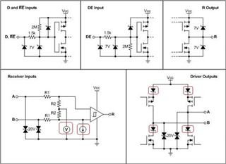
Regarding THVD1550, my customer has additional questions about Equivalent Input and Output Schematic Diagrams.
I would be grateful if you could advise.
---
In the attached document,
Please tell me about the part marked in red.
(1) What is the function of the symbol on the receiver input side? (V and arrow)
(2) Is the zener diode at the driver output 7V like the other blocks?
---
I appreciate your great help in advance.
Best regards,
Shinichi
Hi Shinichi,
For your questions please see below:
(1) V is a biasing voltage and I is a biasing current for receiver that helps set idle characteristics of the receiver.
(2) No the diodes are not 7V - the input at either the A or B terminal is rated +/-15V so these diodes are rated higher than 7V - but we don't specify the exact voltage in the datasheet for these diodes. These diodes are just to prevent backflow of current during driving.
Please let me know if you have any other questions!
Best,
Parker Dodson
Hi Parker,
Thank you for your reply.
I'll share your answer with the customer.
When the customer has an additional question, I consult you again.
I appreciate your great help and cooperation.
Best regards,
Shinichi