This thread has been locked.

If you have a related question, please click the "Ask a related question" button in the top right corner. The newly created question will be automatically linked to this question.

DS90UB947-Q1EVM: I2C back channel CRC error

Part Number: DS90UB947-Q1EVM
Other Parts Discussed in Thread: ALP

Hi Team,

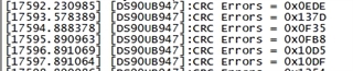
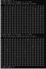
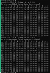
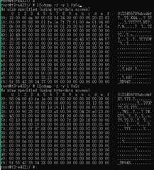
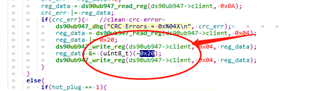
We have another issue:some panel will touch carton,I2C transparent transmission failure with high probability, our engineer already read the 0x0A/0x0B registers of 947 and found many number of back channel CRC errors.

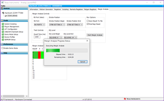
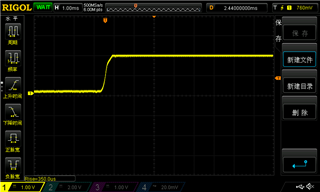
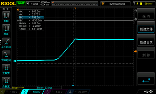
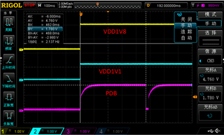
Try to use oscilloscope to measure the 948, the lock single is clear,without any pulses and low level.

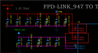
We had do som AB swap, it following with 947.

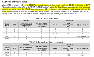
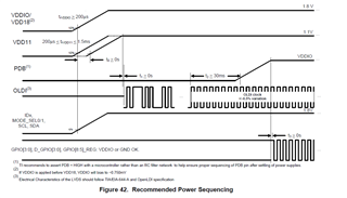
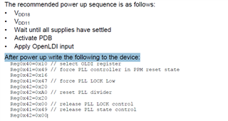
We check the datasheets of 947 and 948, it does not have any describes of back channel, so can you give us some suggestion about this issue?

Best Regards!

  • Sorry, i forgot to upload the log.

  • Hi Yao,

    Thanks for submitting the question. I will review all the details and get back to you when I get a chance, thanks. 

    Regards,
    Fadi A.

  • Hi Fadi,

    Looking forward to your reply,thanks.

    Best Regards.

  • Hey Yao,

    1. How many ICs with this issue are you seeing?
    2. Is this a new application you are designing or you are using TI EVMs?
    3. When you say you did AB swap and it followed 947. Do you mean you replaced the initial 947 IC with a different 947 IC and the issue went away? 
    4. What's the failure rate?
    5. Can you provide a register dump of 947 side and 948 side of a good run vs. a bad run?

    If you aren't getting lock on the Des (948) side. Please see 948 datasheet below. It highlights the different states at which Lock is low vs. high. 

  • Hi Fadi,

    1.10 ICs we had seen this issue;

    2.It is a new application;

    3.I very sorry about this,may be it does not follow 947;

    4.The failure rate is very hard to count,different module's rate is not the same;

    5.The Lock Pin of 948 is always at high level;

    The swap test(host A/B, screen C/D):

    1)A+C:a lot number of back channel CRC errors can be read form the 0x0A/0x0B registers of 947, 948's lock pin is high level, touch panel can not work.

    2)B+C:some back channel CRC errors can be read form the 0x0A/0x0B registers of 947, the failture rate is lower than A+C, touch panel work normally.

    3)A+D:without  any back channel CRC errors,touch panel work normally.

    Is any suggestions can help we debug this back channel CRC error?

    Best Regards.

  • Hi Yao,

    Thanks for the info. I will review and get back to you.

    Regards,
    Fadi A.

  • Hi Yao,

    I'm currently out of office. I will review and get back to you no later than Wednesday 11/16.

    Regards,
    Fadi A.

  • Hi Fadi,

    Thank you very much,looking forward to your reply.

    Best Regards.

  • Thank you. Currently out of office, will review and get back to you this week.

  • Hi Fadi,

    I need to deal with this issue urgently, can you ask you colleagues whether they can help me check this issue?

    Best RegardS.

  • Hi Yao,

    Have you tried clearing the Back channel CRC registers after power-up? 

    Typically Back channel CRC errors can accumulate at power-up due to power-supply noise etc. So you need to clear them up after power-up and then check these registers if any errors are accumulated. 

    Regards,
    Fadi A.

  • In addition, can you run MAP tool on the passing Vs. Failing system to analyze your link margin?

    Map tool can be operated from ALP software from the 948 side.

    Click on Margin Analysis tab on ALP software.

    select RX Port0 and select strobe settings 0 to 9

    Select EQ levels 0 to 14 

    Dwell time 1000

    Start Margin analysis.

    Can you send me the results for a good vs. bad system?

    Regards,
    Fadi A.

  • Hi Fadi,

    I had already cleared the bit5 of register 0x04, it did not fix this issue.

    I do not use the MAP Tool before, is any training documents can you supply to me, and where can I download this Tool?

    Best Regards.

  • Hi Yao,

    Here is a link of the MAP tool. It explains how to download and use.

    https://www.ti.com/lit/ug/snlu243/snlu243.pdf?ts=1668562254888&ref_url=https%253A%252F%252Fwww.google.com%252F

    3.I very sorry about this,may be it does not follow 947;

    If the issue is not following 947 then it's not likely that FPD-Link IC is causing the issue.

    Can you send me your schematic for review? Do all the failing and passing systems have the same application design? 

    If not send me the schematic for a failing system and a passing system I can look to see if anything is abnormal. 

    1)A+C:a lot number of back channel CRC errors can be read form the 0x0A/0x0B registers of 947, 948's lock pin is high level, touch panel can not work.

    If Lock is high that means valid data and clock are recovered from the serial input of the 948 and it is available on the LVCMOS and LVDS outputs, so no issue on FPD-Link Ser/Des ICs link. 

    Regards,
    Fadi A.

  • Hi Fadi,

    The schematic is encrypted, I will try to decrypt it if my boss agree.

    The failing module and passing module are the same design.

    My colleague will try to use the MAP Tool for debug.

    Best Regards.

  • Hi Fadi,

    This is the power sequencing of 947, is it OK?

  • Hey Yao,

    Can you please capture VDDIO/VDD18/VDD11/PDB in a single scope shot? 

    can you also measure the rise time of each VDD ?

    Are you following the recommended power up sequence init code?

    The schematic is encrypted, I will try to decrypt it if my boss agree.

    If you can't share, please make sure you have the correct configuration on the following:

    • Correct coax/STP mode strapped on both sides Ser/Des
    • Correct AC coupling caps for the cable mode
    • Does this application use PoC?

    Regards,
    Fadi A.

  • Hi Fadi,

    Sorry for delay, VDDIO and VDD18 is the same network:

    This is the VDD11,the rise time is almost 153us-200us:

    This is the VDD18(VDDIO), the rise time is almost 350us:

    And this is the recommended power up sequence init code:

    int reg_data;

    reg_data = ds90ub947_read_reg(ds90ub947->client, 0x03);
    reg_data = reg_data | 0x08;

    ds90ub947_write_reg(ds90ub947->client, 0x03, reg_data);
    ds90ub947_write_reg(ds90ub947->client, 0x4F, 0x80);
    ds90ub947_write_reg(ds90ub947->client, 0x07, 0x34);
    ds90ub947_write_reg(ds90ub947->client, 0x08, 0x34);
    ds90ub947_write_reg(ds90ub947->client, 0xC6, 0x21);
    ds90ub947_write_reg(ds90ub947->client, 0x1E, 0x04);
    ds90ub947_write_reg(ds90ub947->client, 0x0D, 0x03);//GPIO0
    ds90ub947_write_reg(ds90ub947->client, 0x0E, 0x33);
    ds90ub947_write_reg(ds90ub947->client, 0x0F, 0x03);
    ds90ub947_write_reg2(ds90ub947->client, 0x0D, 0x05);//DGPIO0

    ds90ub947_write_reg(ds90ub947->client, 0x40, 0x10);
    ds90ub947_write_reg(ds90ub947->client, 0x41, 0x4a);
    ds90ub947_write_reg(ds90ub947->client, 0x42, 0x3f);
    ds90ub947_write_reg(ds90ub947->client, 0x41, 0x4b);
    ds90ub947_write_reg(ds90ub947->client, 0x42, 0x88);
    ds90ub947_write_reg(ds90ub947->client, 0x41, 0x49);
    ds90ub947_write_reg(ds90ub947->client, 0x42, 0x10);
    msleep(10);
    ds90ub947_write_reg(ds90ub947->client, 0x42, 0x00);

    ds90ub947_write_reg(ds90ub947->client, 0x40, 0x14);
    ds90ub947_write_reg(ds90ub947->client, 0x41, 0x4a);
    ds90ub947_write_reg(ds90ub947->client, 0x42, 0x3f);
    ds90ub947_write_reg(ds90ub947->client, 0x41, 0x4b);
    ds90ub947_write_reg(ds90ub947->client, 0x42, 0x88);
    ds90ub947_write_reg(ds90ub947->client, 0x41, 0x49);
    ds90ub947_write_reg(ds90ub947->client, 0x42, 0x10);
    msleep(15);
    ds90ub947_write_reg(ds90ub947->client, 0x42, 0x00);

    msleep(10);
    ds90ub947_write_reg(ds90ub947->client, 0x40, 0x10);
    ds90ub947_write_reg(ds90ub947->client, 0x41, 0x49);
    ds90ub947_write_reg(ds90ub947->client, 0x42, 0x16);
    ds90ub947_write_reg(ds90ub947->client, 0x41, 0x47);
    ds90ub947_write_reg(ds90ub947->client, 0x42, 0x20);

    ds90ub947_write_reg(ds90ub947->client, 0x42, 0xA0);

    ds90ub947_write_reg(ds90ub947->client, 0x42, 0x20);
    ds90ub947_write_reg(ds90ub947->client, 0x42, 0x20);
    ds90ub947_write_reg(ds90ub947->client, 0x42, 0x20);
    ds90ub947_write_reg(ds90ub947->client, 0x42, 0x20);
    ds90ub947_write_reg(ds90ub947->client, 0x42, 0x20);
    msleep(5);
    ds90ub947_write_reg(ds90ub947->client, 0x42, 0x00);
    msleep(5);
    ds90ub947_write_reg(ds90ub947->client, 0x41, 0x49);
    ds90ub947_write_reg(ds90ub947->client, 0x42, 0x00);
    msleep(5);

    Best Regards.