


Part Number: SN65MLVD206B
Several years ago a question was asked regarding glitches on the receive output pin of a receiving node when DE transitions from high to low (https://e2e.ti.com/support/interface-group/interface/f/interface-forum/126882/help-with-noise-on-a-half-duplex-m-lvds-line) on a transmitting node. The last post by Earl Close describes my exact same situation with the SN65MLVD206B. My setup is exactly the same. My bus cabling is 100 ohm twisted shielded pair with 100 ohm termination on both ends. *RE is permanently asserted on all nodes.
When a node is finished transmitting, the data is logic low (this is our stop bit). When DE is de-asserted (high to low), we see a very brief glitch on the R pin (which should be logic low) of the other nodes on the bus. At the DE transition, we see both A and B lines begin their transition to a floating state, but for a very brief amount of time, A rises slightly above B causing the logic high glitch on the R pins. We tried to add a resistor bias network on the bus to pull A low and B high during idle, but found that we had to implement this on every node right at the device A and B pins.
Just wanted to re-post the issue to see if there might be any suggestions of what could be happening.
Below is the original question posted in the now closed thread:
I am having the exact same problem as Luis. I am using the 65MLVD206 and tried briefly with the 65MLVD201 to see if it was better. My setup has a transmitter at one end (switched on and off via TE), 10 cm of transmission line, and a receiver at the other end. *RE is tied low at both ends. Each end has a 100 ohm terminator. I need R at the receiving end to look exactly like D at the transmitting end. I will show you what I found on the scope:

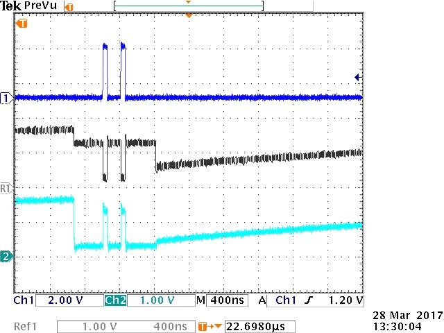
1: signal at D on transmitting 65MLVD206
R2: signal at R on receiving 65MLVD201 (not really usable)
2: signal at R on receiving 65MLVD206 (this has the glitch when TE is turned off)
R1: signal at DE on transmitting 65MLVD206
Zooming in on the glitch on the R line (the bottom trace):
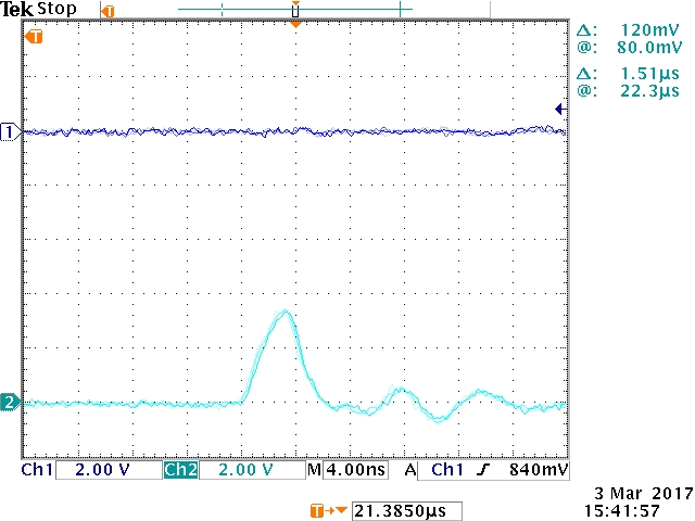
and looking at the LVDS A and B lines:
1: signal at D on transmitting 65MLVD206
R1: signal at B on receiving 65MLVD206
2: signal at A on receiving 65MLVD206
From this you can see that the LVDS signals behave. When TE is turned off, the B signal rapidly drops, and the A line moves up slightly but still B>A so we should not see a 1 output.
It seems if I go to a 50 ohm termination instead of 100 ohm the problem goes away. I can also bias as Luis did, but it seems something is fundamentally wrong. I want a robust solution, and I fear this is a band-aid solution.
Are you able to explain what is happening? Does the receiver have some inductance such that when B drops rapidly with A rising that it sees this as a 1, even though the voltage levels don't justify this?
Thanks,
Earl
