This thread has been locked.

If you have a related question, please click the "Ask a related question" button in the top right corner. The newly created question will be automatically linked to this question.

DS90UH941AS-Q1: Pattern initialization parameters for 941AS+928Q and power-up timing control

Part Number: DS90UH941AS-Q1
Other Parts Discussed in Thread: DS90UB928Q, ALP, USB2ANY

Hi team,

One of our customer's issues, I'm forwarding it below, could you please provide some guidance?

Scenario:

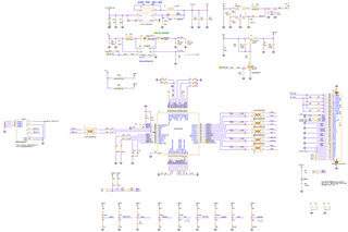
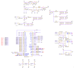
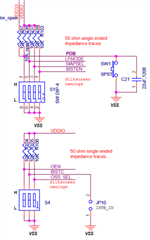
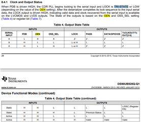
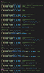
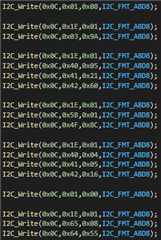
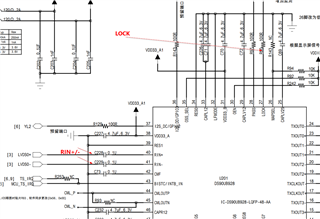
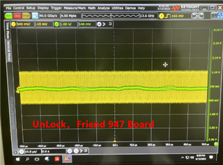
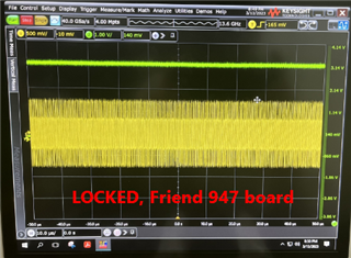
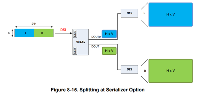
Enter 2560x768 stitching RGB888 data to DS90UH941AS-Q1 using one MIPI DSI4lane and divided into two serial signals of 1280x768 via the internal splitter, each of which is input into two DS90UB928Q.It is deserialized and converted into LVDS signals, which are output to two LVDS panels respectively. As shown in the following figure of the datasheet.

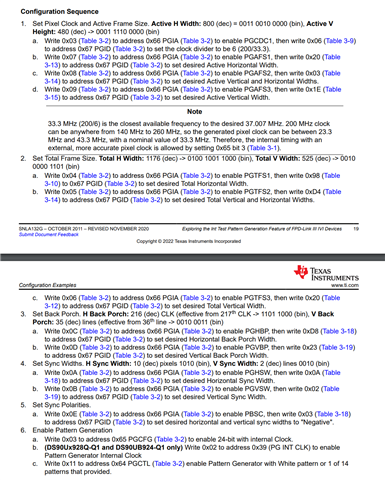
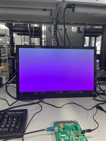
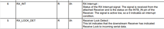
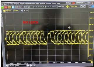
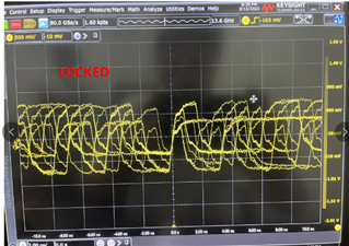
1, MIPI DSI two 1280x768 splice not complete, can 941AS Pattern generator generate two 1280x768 serial signal output for debugging screen use?

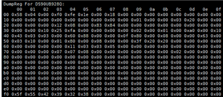
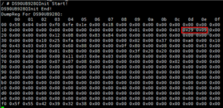
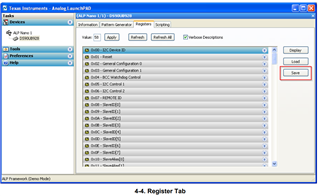
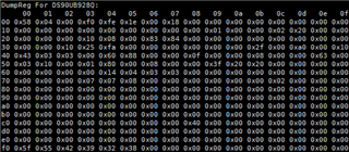
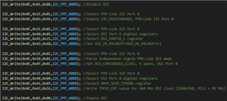
2, 941AS and 928Q, are there tools to generate a list of initialization parameters that meet the power-up timing requirements?

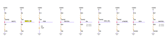
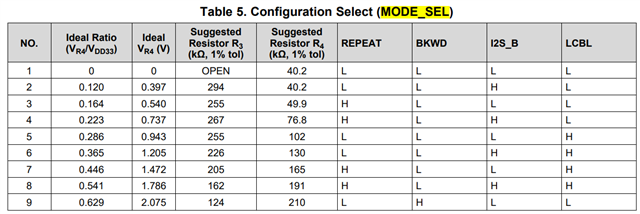
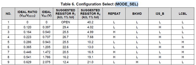
3, whether the LVDS screen needs to be illuminated by 2:2 single pattern first, how to configure the initialization parameters of 941AS and 928Q

Best Regards,

Amy Luo

  • Hi Amy,

    1.) The 941AS does come with two different PatGen blocks, so you should be able to generate two different patterns. Is ALP being used? If ALP is being used, the pattern generator section under the 941AS Profile should have a PatGen Select option at the bottom. Using this, you should be able to tab between the two different patterns being sent out and verify whether the output and screens work.

    2&3.) What do you mean by initialization parameters? Do you mean enabling splitter mode, PatGen, and register values at start up? Or do you mean ensuring the correct power-up timings during the power up sequence to make sure the device functions? 

    Additionally, could you possibly provide more information regarding the customers setup? Such as the Active Video Resolutions, the PCLK rate and the DSI clock rate, and the DSI mode being used? I would appreciate it!

    Thanks,

    Ryan

  • Hi Ryan,

    Thank you for your kindly support.

    I got feedback from customers like the following:

    The initialization parameters mean the register configuration of the 941AS/928Q output test Pattern. I recommended the snla132g.pdf document to my customer. The customer refers to the instructions in the documentation to set the 928Q Pattern register related parameters as follows.
    But the Panel does not show any, the timing meets the requirements of the Panel, all using 928Q internal CLK, please help to confirm whether the 0x64/0x65/0x39 register is set correctly. Are there any other registers that need to be programmed in addition to the following, such as the Reset control in 0x01, etc.?

        //Internal CLK DIV
        I2C_Write(0x2C,0x66,0x03,I2C_FMT_A8D8); //Addr
        I2C_Write(0x2C,0x67,0x03,I2C_FMT_A8D8); //Data

        //HActive LSB
        I2C_Write(0x2C,0x66,0x07,I2C_FMT_A8D8); //Addr
        I2C_Write(0x2C,0x67,0x00,I2C_FMT_A8D8); //Data

        //HActive MSB& VActive LSB
        I2C_Write(0x2C,0x66,0x08,I2C_FMT_A8D8); //Addr
        I2C_Write(0x2C,0x67,0x05,I2C_FMT_A8D8); //Data
        //VActive MSB
        I2C_Write(0x2C,0x66,0x09,I2C_FMT_A8D8); //Addr
        I2C_Write(0x2C,0x67,0x30,I2C_FMT_A8D8); //Data

        //HTotal LSB
        I2C_Write(0x2C,0x66,0x04,I2C_FMT_A8D8); //Addr
        I2C_Write(0x2C,0x67,0x72,I2C_FMT_A8D8); //Data
        //HTotal MSB& VTotal LSB
        I2C_Write(0x2C,0x66,0x05,I2C_FMT_A8D8); //Addr
        I2C_Write(0x2C,0x67,0x26,I2C_FMT_A8D8); //Data
        //VTotal MSB
        I2C_Write(0x2C,0x66,0x06,I2C_FMT_A8D8); //Addr
        I2C_Write(0x2C,0x67,0x33,I2C_FMT_A8D8); //Data

        //HBP
        I2C_Write(0x2C,0x66,0x0C,I2C_FMT_A8D8); //Addr
        I2C_Write(0x2C,0x67,0xA0,I2C_FMT_A8D8); //Data
        //VBP
        I2C_Write(0x2C,0x66,0x0D,I2C_FMT_A8D8); //Addr
        I2C_Write(0x2C,0x67,0x18,I2C_FMT_A8D8); //Data

        //HSW
        I2C_Write(0x2C,0x66,0x0A,I2C_FMT_A8D8); //Addr
        I2C_Write(0x2C,0x67,0x24,I2C_FMT_A8D8); //Data
        //VSW
        I2C_Write(0x2C,0x66,0x0B,I2C_FMT_A8D8); //Addr
        I2C_Write(0x2C,0x67,0x04,I2C_FMT_A8D8); //Data

        //POL&HV_DIS
        I2C_Write(0x2C,0x66,0x0E,I2C_FMT_A8D8); //Addr
        I2C_Write(0x2C,0x67,0x00,I2C_FMT_A8D8); //Data

        //FPS
        I2C_Write(0x2C,0x66,0x0F,I2C_FMT_A8D8); //Addr
        I2C_Write(0x2C,0x67,0x18,I2C_FMT_A8D8); //Data

        I2C_Write(0x2C,0x65,0x03,I2C_FMT_A8D8); //
        I2C_Write(0x2C,0x39,0x02,I2C_FMT_A8D8); //
        I2C_Write(0x2C,0x64,0x51,I2C_FMT_A8D8); //
    The customer has confirmed that the Panel hardware connection is good and the screen can output various patterns using the Panel's own self-test mode.
    Use the Pattern signal from the 928Q to the Panel to test that there is no picture output.
    PASS pin is Low, LOCK pin is High

    Best Regards,

    Amy

  • Hi Amy,

    I am looking over this data, and I am looking at how we can copy these settings onto a test on our side to see if we can replicate this and solve the issue, and I will try to get an answer to you by the end of the week at the latest, 2/3.

    If any other info or questions pop up, feel free to let me know.

    Thanks,

    Ryan

  • Hi Ryan,

    Thanks for your response.  Below is the follow-up question for this customer, please give your comments.

    I have confirmed that the 928Q VDD33/VDDIO and other power supplies have 3.3V, RTERM = 100Ω, please help to confirm the following pin design is correct, MODE_SEL corresponds to R4 = 1.354V R6 = 2.046V, is there a problem?

    Based on my current usage scenario: Only one LVDS Panel per 928Q is illuminated and there is no audio transmission requirement, MODE_SEL should be configured to which of the following sets?

    Completely copy snla132g.pdf document this set of initialization parameters, just modify the corresponding internal 200M for 160M calculation PCLK (928Q built-in clock source is 160M), other are set according to the parameters in the screenshot below, do not connect LVDS screen, measuring LVDS output, LVDS CLK/DATA Lane are only high and low level changes, no LVDS signal waveform is available.

        //Internal CLK DIV
        I2C_Write(0x2C,0x66,0x03,I2C_FMT_A8D8); //Addr
        I2C_Write(0x2C,0x67,0x05,I2C_FMT_A8D8); //Data

        //HActive LSB
        I2C_Write(0x2C,0x66,0x07,I2C_FMT_A8D8); //Addr
        I2C_Write(0x2C,0x67,0x20,I2C_FMT_A8D8); //Data

        //HActive MSB& VActive LSB
        I2C_Write(0x2C,0x66,0x08,I2C_FMT_A8D8); //Addr
        I2C_Write(0x2C,0x67,0x03,I2C_FMT_A8D8); //Data
        //VActive MSB
        I2C_Write(0x2C,0x66,0x09,I2C_FMT_A8D8); //Addr
        I2C_Write(0x2C,0x67,0x1E,I2C_FMT_A8D8); //Data

        //HTotal LSB
        I2C_Write(0x2C,0x66,0x04,I2C_FMT_A8D8); //Addr
        I2C_Write(0x2C,0x67,0x98,I2C_FMT_A8D8); //Data
        //HTotal MSB& VTotal LSB
        I2C_Write(0x2C,0x66,0x05,I2C_FMT_A8D8); //Addr
        I2C_Write(0x2C,0x67,0xD4,I2C_FMT_A8D8); //Data
        //VTotal MSB
        I2C_Write(0x2C,0x66,0x06,I2C_FMT_A8D8); //Addr
        I2C_Write(0x2C,0x67,0x20,I2C_FMT_A8D8); //Data

        //HBP
        I2C_Write(0x2C,0x66,0x0C,I2C_FMT_A8D8); //Addr
        I2C_Write(0x2C,0x67,0xD8,I2C_FMT_A8D8); //Data
        //VBP
        I2C_Write(0x2C,0x66,0x0D,I2C_FMT_A8D8); //Addr
        I2C_Write(0x2C,0x67,0x23,I2C_FMT_A8D8); //Data

        //HSW
        I2C_Write(0x2C,0x66,0x0A,I2C_FMT_A8D8); //Addr
        I2C_Write(0x2C,0x67,0x0A,I2C_FMT_A8D8); //Data
        //VSW
        I2C_Write(0x2C,0x66,0x0B,I2C_FMT_A8D8); //Addr
        I2C_Write(0x2C,0x67,0x02,I2C_FMT_A8D8); //Data

        //POL&HV_DIS
        I2C_Write(0x2C,0x66,0x0E,I2C_FMT_A8D8); //Addr
        I2C_Write(0x2C,0x67,0x03,I2C_FMT_A8D8); //Data

        I2C_Write(0x2C,0x65,0x03,I2C_FMT_A8D8); //
        I2C_Write(0x2C,0x39,0x02,I2C_FMT_A8D8); //
        I2C_Write(0x2C,0x64,0x11,I2C_FMT_A8D8); //
    Best Regards,
    Amy Luo
  • Hi Amy,

    Mode_Sel should be chosen by what is needed for the system, I.E HDCP, Backwards Compatibility, LCBL Mode, and I2S_Surround audio settings. Depending on what they need, they should also make sure the resistors follow the indicated ratio for that setting. From how its setup now, it seems like they are going for setting 9. If HDCP is not being used and there is no audio requirement, then I believe setting 2 could work. But again, that depends on customer config.

    For the PatGen code, is patgen being run from the deserializer or the serializer? The address being used in the code leads me to believe deserializer, but if otherwise, remember that the section exclusive to 928 PatGen wouldn't be necessary. Additionally, what is being used to execute the script? ALP or a separate I2C GUI?

    The settings described in the app note are for an 800X480 image, as long as the display it is going to has no issue with that, the script described by the app note should work. If you are seeing the LOCK pin go high, then that should indicate that PatGen and outputs should be enabled. If possible, monitor the output of the LOCK pin and verify that it is driven high and not being changed.

    Thanks,

    Ryan

  • Dear Ryan,

    Thinks for your response

    1、The PatGen code is running from the deserializer (DS90UB928Q), I executed the script use a separate I2C host device , not use ALP. The LOCK PIN have is high, but the TxCLKOUT/TxOUT Pin without LVDS signal output. 

    2、Write  0x09 into  reg(0x1D) &reg(0x1E)of 928Q  as blow,but the GPIO0/GPIO1 can't output high,

        I2C_Write(0x2C,0x1D,0x09,I2C_FMT_A8D8); //GPIO0 Output High

        I2C_Write(0x2C,0x1E,0x09,I2C_FMT_A8D8); //GPIO1 Output High
       I have read the reg(0x1D) &reg(0x1E)and  confirmed the 0x09 has write isuccessfully.
    3、Can you help me check the schematic diagram of 928Q as blow,
  • Hi Gene and Amy,

    First, is the 928Q being written and read locally, or are they being read remotely via the 941AS?

    Next, double check that all the registers being written to are in fact changing their values, as well as reading the 0x00 register to see what the device ID is.

    Also, if you could also supply the 941AS schematic, I would appreciate it. I will continue looking at the 928 schematic, but so far I have not seen any issues.

    One thing I am worried about is the device IDs. Please make sure that each serializer and deserializer has a unique ID assigned to them via the IDx pin. Having multiple devices with the same ID may cause issues with reading and writing to registers.

    From what I can tell in the commands, it does seem like they should be having an effect on the outputs, so its strange that they are not. I will look into whether we have seen anything like this before.

    Thanks,

    Ryan

  • Dear Ryan

    1、928Q is being written and read locally,the I2C 7bit DeviceID is 0x2C,and I used different I2C master device to control the 928Q and 941AS.

    2、928Q reg(0x00)=0x58, all direct registers value dump as blow:

    3、941AS-Q schematic as blow,the I2C 7bit DeviceID 0x0C:

  • Hi Gene,

    Thanks, I appreciate it. I'll take a look at this info and try to get answer to you regarding what we can figure out by the the beginning of next week at the latest.

    Thanks,

    Ryan

  • Hi Gene,

    Seems like the schematic for the 941-AS is good as well, though I want to confirm that STP is being used, not coax.

    For the 928 schematic, I did notice that there are grounds attached to the Vddio and Vdd3v3 pins, I just wanted to confirm that there power sources are properly connected, and that those are just errors on the schematic.

    I also noticed that, with the Mode_Sel on the 928, the Mode_Sel voltage is 1.98, which is not spec'd towards any specific level. If possible, please use the resistors indicated on the table to ensure correct voltage levels.

    With this register dump, is it from before changing the value of the GPIO registers or after?

    Have you tried replicating this issue with a different 928 or different serializer? 

    I will try to align with the team internally to see if anyone else has any insight on this issue, as well as trying to get a setup going on our side to see if we can replicate this with our EVMs and I will see if I can figure anything out.

    Thanks,

    Ryan

  • Dear Ryan,

    Thanks for your reply,

    1、I have confirmed the 941AS connect 928 used STP .

    2、VDDIO/VDD33 = 3.368V ,they are not attached to ground ,there is  a 4.7uF capacity between VDDIO/VDD33 pin and groud.

    3、I change the resistor R3 = 124kΩ,R4 = 210kΩ,VR4 = 2.112V,VR4/VDD33 = 0.627, MODE_SEL is NO.9, still not have LVDS signal output.

    4、This register dump after changing the value of the GPIO registers

    5、We have tried 2 pcs of 928Q PCBA, they are same. 

  • Hi Gene,

    4、This register dump after changing the value of the GPIO registers

    If this is the case, then I don't see any changes being made to the GPIO registers, 0x1D and 0x1E. GPIO 0 and 1 both look like they are inactive and have not been written to. Can you confirm that this is consistent by again writing to those GPIO registers and dumping the registers again or reading them?

    Would it be possible to send video timings and properties? I need them to get PatGen going on our side.

    Thanks,

    Ryan

  • Dear Ryan,

    The picture of dump register  above is not set   0x1D,0x1E register.

    the all  registers setting code and dump value as blow:

  • Dear Ryan,

    After we changed MODE_SEL = NO.0,   OSS_SEL changed to high level,

    I write  0x09 into  reg(0x1D) &reg(0x1E)of 928Q  as blow,but the GPIO0/GPIO1 can output high,,and write  0x01 into  reg(0x1D) &reg(0x1E)of 928Q  as blow,but the GPIO0/GPIO1 can output low,but no LVDS signel output yet.

     
    The PIN value test by Oscilloscope as blow:
    PDB OEN OSS_SEL LOCK PASS TxCLKOUT/TxOUT[3:0]
    High High High High High(3.3V) 1.2V
  • Hi Gene,

    So to confirm, after switching to Mode 1 instead of Mode 9, you were able to see high/low signals coming from the GPIO as intended?

    This makes sense, as backward-compatible mode, which is enabled in mode 9, disables many features, including bidirectional GPIOs.

    You also switched OSS_SEL to high? That should be good as well.

    If possible, could you install ALP and see if you can use that with the 928 locally to enable PatGen on the 928 and see if you have the same results? From my end, I have a 941AS-EVM and 928EVM connected using the PatGen function with internal timing via ALP, and I can see output from the TxOUT pins.

    Thanks,

    Ryan

  • Hi Ryan,

    I don't have USB2ANY device to connect my board to ALP PC tool,can you provide the registors parameter of 941AS and 928Q you used to me?

    I find  this file DS90UB928QEVM User Guide (ti.com.cn),you can save the registors to a file ,can save your test registors parameter to me?

    Can you draw a picture for me to show the S1/S4/S5(PDB/LFMODE/MAPSEL/BISTEN/OEN/BISTC/OSS_SEL/MODE_SEL)  status,

    i want to change my board same as EVM ,and use the registor parameters you used .

  • Hi Gene,

    Here are some pictures to illustrate the setup of our EVM, as well as a register dump from ALP.

    2_17_928EVM_RegisterSave.txt
    [REGISTERS]
    Device = ALP Nano 1 - DS90UB928, Connector 1
    Comments = "Results from 2/17 PatGen tests"
    Date = 02/17/2023
    Time = 14:54:18
    Reg = 0,0x0000,0x58
    Reg = 0,0x0001,0x04
    Reg = 0,0x0002,0x00
    Reg = 0,0x0003,0xF0
    Reg = 0,0x0004,0xFE
    Reg = 0,0x0005,0x1E
    Reg = 0,0x0006,0x80
    Reg = 0,0x0007,0x18
    Reg = 0,0x0008,0x00
    Reg = 0,0x0009,0x00
    Reg = 0,0x000A,0x00
    Reg = 0,0x000B,0x00
    Reg = 0,0x000C,0x00
    Reg = 0,0x000D,0x00
    Reg = 0,0x000E,0x00
    Reg = 0,0x000F,0x00
    Reg = 0,0x0010,0x00
    Reg = 0,0x0011,0x00
    Reg = 0,0x0012,0x00
    Reg = 0,0x0013,0x00
    Reg = 0,0x0014,0x00
    Reg = 0,0x0015,0x00
    Reg = 0,0x0016,0x00
    Reg = 0,0x0017,0x00
    Reg = 0,0x0018,0x00
    Reg = 0,0x0019,0x01
    Reg = 0,0x001B,0x00
    Reg = 0,0x001C,0x03
    Reg = 0,0x001D,0x20
    Reg = 0,0x001E,0x00
    Reg = 0,0x001F,0x00
    Reg = 0,0x0020,0x00
    Reg = 0,0x0021,0x00
    Reg = 0,0x0022,0x00
    Reg = 0,0x0023,0x10
    Reg = 0,0x0024,0x08
    Reg = 0,0x0025,0x00
    Reg = 0,0x0026,0x83
    Reg = 0,0x0027,0x84
    Reg = 0,0x0028,0x21
    Reg = 0,0x0029,0x00
    Reg = 0,0x002A,0x00
    Reg = 0,0x002B,0x0C
    Reg = 0,0x0035,0x00
    Reg = 0,0x0039,0x00
    Reg = 0,0x003A,0x00
    Reg = 0,0x003B,0x05
    Reg = 0,0x0041,0x03
    Reg = 0,0x0044,0x60
    Reg = 0,0x0045,0x88
    Reg = 0,0x0049,0x00
    Reg = 0,0x004B,0x08
    Reg = 0,0x0056,0x08
    Reg = 0,0x0064,0x14
    Reg = 0,0x0065,0x04
    Reg = 0,0x0066,0x03
    Reg = 0,0x0067,0x03
    Reg = 0,0x006E,0x00
    Reg = 0,0x006F,0x00
    Reg = 0,0x00F0,0x5F
    Reg = 0,0x00F1,0x55
    Reg = 0,0x00F2,0x42
    Reg = 0,0x00F3,0x39
    Reg = 0,0x00F4,0x32
    Reg = 0,0x00F5,0x38
    

    I also tested with OEN, OSS_SEL, and OEN/OSS_SEL Override enabled, and I was still able to see activity in the TxOut lanes.

    Let me know if you are able to see comparable results!

    Also, as a heads up, we will be OoO next Monday, 2/20, due to a National Holiday, so responses will likely be delayed to 2/21.

    Thanks,

    Ryan

  • Hi,Ryan,

    It's also no LVDS signal output .

    Which select is right ,the OEN/OSS_SEL Status as below:

    the register(0x02) is 0x00, LVCMOS Output is disable ?

  • Hi Gene,

    OEN affects whether LVCMOS output in enabled or not. when low, LVDS should be the main output.

    OSS_SEL controls what the output of the device is when lock is low.

    If the intended output of this device is LVDS, then I do not believe the setting for OEN or OSS_SEL matters, but I will ask internally if anyone has any contradictory info.

    One thing I do want to try is two lines of script. Using these two lines, I am able to enable patgen, so I want to see if its possible to do this on your side, here are the two lines:

    board.WriteI2C(0x58, 0x64,0x64)

    board.WriteI2C(0x58,0x65,0x04)

    If you can adapt these to work with your I2C and give them a try, see if the TxOUT pins stay at 1.2V or change, I would appreciate it. Again, in the mean time, I will confirm whether the settings of OEN or OSS_SEL are important for LVDS.

    Thanks,

    Ryan

  • Dear Ryan,

    The TxOUT pins stay at 1.2V,

    ...

  • Hi Gene,

    Hmm, Odd. I went ahead and tried the script that can be found on our App Note, and I did notice one issue with it that could be affecting performance. Towards the end of the script, it instructs to write 0x03 to register 0x65 to enable patgen with internal timing. However, writing 0x03 to this register will not enable internal timing, you actually have to write 0x07 to it. I updated the script that Amy sent at the top of the thread to reflect this: 

    928TestScript.txt
      //Internal CLK DIV
        I2C_Write(0x2C,0x66,0x03,I2C_FMT_A8D8); //Addr
        I2C_Write(0x2C,0x67,0x05,I2C_FMT_A8D8); //Data
        //HActive LSB
        I2C_Write(0x2C,0x66,0x07,I2C_FMT_A8D8); //Addr
        I2C_Write(0x2C,0x67,0x20,I2C_FMT_A8D8); //Data
        //HActive MSB& VActive LSB
        I2C_Write(0x2C,0x66,0x08,I2C_FMT_A8D8); //Addr
        I2C_Write(0x2C,0x67,0x03,I2C_FMT_A8D8); //Data
        //VActive MSB
        I2C_Write(0x2C,0x66,0x09,I2C_FMT_A8D8); //Addr
        I2C_Write(0x2C,0x67,0x1E,I2C_FMT_A8D8); //Data
        //HTotal LSB
        I2C_Write(0x2C,0x66,0x04,I2C_FMT_A8D8); //Addr
        I2C_Write(0x2C,0x67,0x98,I2C_FMT_A8D8); //Data
        //HTotal MSB& VTotal LSB
        I2C_Write(0x2C,0x66,0x05,I2C_FMT_A8D8); //Addr
        I2C_Write(0x2C,0x67,0xD4,I2C_FMT_A8D8); //Data
        //VTotal MSB
        I2C_Write(0x2C,0x66,0x06,I2C_FMT_A8D8); //Addr
        I2C_Write(0x2C,0x67,0x20,I2C_FMT_A8D8); //Data
        //HBP
        I2C_Write(0x2C,0x66,0x0C,I2C_FMT_A8D8); //Addr
        I2C_Write(0x2C,0x67,0xD8,I2C_FMT_A8D8); //Data
        //VBP
        I2C_Write(0x2C,0x66,0x0D,I2C_FMT_A8D8); //Addr
        I2C_Write(0x2C,0x67,0x23,I2C_FMT_A8D8); //Data
        //HSW
        I2C_Write(0x2C,0x66,0x0A,I2C_FMT_A8D8); //Addr
        I2C_Write(0x2C,0x67,0x0A,I2C_FMT_A8D8); //Data
        //VSW
        I2C_Write(0x2C,0x66,0x0B,I2C_FMT_A8D8); //Addr
        I2C_Write(0x2C,0x67,0x02,I2C_FMT_A8D8); //Data
        //POL&HV_DIS
        I2C_Write(0x2C,0x66,0x0E,I2C_FMT_A8D8); //Addr
        I2C_Write(0x2C,0x67,0x03,I2C_FMT_A8D8); //Data
    
        I2C_Write(0x2C,0x65,0x07,I2C_FMT_A8D8); //
        I2C_Write(0x2C,0x39,0x02,I2C_FMT_A8D8); //
        I2C_Write(0x2C,0x64,0x11,I2C_FMT_A8D8); //

    After making that change, I ran the script on my side and could see patgen coming from the 928.

    I would ask that you give that a try and see if you notice anything, if not, its possible that there could be an issue with how I2C commands are being sent to the indirect registers or perhaps something else in the testing process.

    Thanks,

    Ryan

  • Dear ryan,

    Thanks, I have no new info sync to you,I will ask a local friend who has ported the 928Q successfully help me check first.

    When i have new message ,i sync to you in time.

  • Hi Gene,

    Ok, sounds good. Yes, let me know what you here from your local friend when you have more info.

    Thanks,

    Ryan

  • Dear Ryan,

    I borrowed a 928Q and 947Q board from my friend, the same registers table can't show pattern on the panel too, but his 947Q can send pattern signal to the 928Q board, the panel after 928Q can show the pattern success. The 974Q and 928Q connected with STP,so I try to do use my 941AS-Q send pattern signal to the good 928Q board, but it's failed too. Do you have any suggests?

    I Read the all status registors as blow,

    the GENERAL_STS(0x0C) register shows "Cable link not detected"

    the STS(0xC4) register shows "RX_INT not active"

    I2C_Read GENERAL_STS:0x00

    I2C_Read TX_MODE_STS:0x8B

    I2C_Read BCC_STATUS:0x00

    I2C_Read STS:0x40

    I2C_Read DPHY_STATUS:0x1F

    I2C_Read DPHY_DLANE0_ERR:0x00

    I2C_Read DPHY_DLANE1_ERR:0x00

    I2C_Read DPHY_DLANE2_ERR:0x00

    I2C_Read DPHY_DLANE3_ERR:0x00

    I2C_Read DPHY_ERR_CLK_LANE:0x00

    I2C_Read DPHY_SYNC_STS:0x00

    I2C_Read DSI_ERR_CFG_0:0xFF

    I2C_Read DSI_ERR_CFG_1:0x7F

    I2C_Read DSI_STATUS:0x00

    I2C_Read DSI_ERR_COUNT:0x00

    I2C_Read DSI_VC_DTYPE:0x00

    I2C_Read DSI_ERR_RPT_0:0x00

    I2C_Read DSI_ERR_RPT_1:0x00

    I2C_Read DSI_ERR_RPT_2:0x00

  • Hi Gene,

    Going by the GENERAL_STS register, it sounds like 941AS is not able to connect to the 928. Since the 947 was seemingly able to, I would say that this sounds like a hardware issue.

    Double-check that the Power-up sequence is not being violated, that there is pin-continuity, and that there are no open caps.

    Thanks,

    Ryan

  • Dear Ryan,

    I checked the hardware,  not find any error .the DOUT0_P/N of 941AS-Q has serial signal output,

    the GENERAL_STS(0x0C) register shows PCLK_DETECT is active when i use DSI CLK ,but LINK_DETECT is 0 too.

    the STS(0xC4) register shows "RX_INT not active" , the right value of STS is "0x28" ?

    RX_INT active is need to pull down the INTB_IN PIN of 928Q?

    I2C_Read GENERAL_STS:0x04

    I2C_Read TX_MODE_STS:0x8B

    I2C_Read BCC_STATUS:0x00

    I2C_Read STS:0x40

    I2C_Read DPHY_STATUS:0x1F

    I2C_Read DPHY_DLANE0_ERR:0x00

    I2C_Read DPHY_DLANE1_ERR:0x00

    I2C_Read DPHY_DLANE2_ERR:0x00

    I2C_Read DPHY_DLANE3_ERR:0x00

    I2C_Read DPHY_ERR_CLK_LANE:0x00

    I2C_Read DPHY_SYNC_STS:0x00

    I2C_Read DSI_STATUS:0x00

    I2C_Read DSI_ERR_COUNT:0x00

    I2C_Read DSI_VC_DTYPE:0x00

    I2C_Read DSI_ERR_RPT_0:0x00

    I2C_Read DSI_ERR_RPT_1:0x00

    I2C_Read DSI_ERR_RPT_2:0x00

  • Hi Gene,

    Did you also check the hardware of both 928s?

    Yes, the value of the STS register should be 0x28. On the 941AS, the RX_INT bit of the STS register is used to indicate when the INTB_IN pin of the attached deserializer is active, it does not need to be to be active for functionality.

    One thing I noticed after looking at the value of the TX_MODE_STS register value, it reads out 8B, even though when looking at the schematic, it should read out as 8F. I just want to confirm, did you adjust the resistors for MODE_SEL0 to disable splitter mode on the 941AS?

    For MODE_SEL1, which setting is being used on the 941AS? Is CLOCK enabled or disabled?

    Do you still have your friends 947 and 928 boards? If so, could you compare these same registers and see if the STS and GENERAL_STS see the link and indicate it via their register bits?

    Is the schematic of the good 928Q board similar? would it be possible to send it?

    Thanks,

    Ryan

  • Dear Ryan,

    1、When connect to 947 board, the 928 board is good , change the STP connect from to 941 board, can't show anything.

    ->Yes.I changed the MODE_SEL0 = mode 3,MODE_SEL1 = mode 0 ,so TX_MODE_STS = 0x8B is right. the CLOCK enabled

    2、The register(0x56)  set to 0x02,in the internal clk,GENERAL_STS(0x0C) register shows PCLK_DETECT is active,same as DSI clk.but Cable link fail too,.and the 928Q LOCK PIN can't pull up.

    I check the 7 cases of link fault, not find any issue

    3、The INTB PIN is not important for the colorbar output?It's only used for customer function?

    I have compared the registers with my friend's 928Q board,is same as mine,but his board MCU will pulldown the INTB_IN ,my board not do it. his board not open the debug port to me,so I can't get the realtime value of the registers . I don't know when i should pulldown the INTB_IN of 928Q and  INTB_IN of  941AS, after i2c init ,or before i2c init? the register  0xC6[5] = 1 and 0xC6[0] = 1 is must be set? 

    4、The schematic of  928Q board is as blow,I don't the schematic of 947 board 

    BU928.pdf

  • Hi Gene,

    1.) Would it be possible to monitor the the CLK (REFCLK, DSIx_CLK) pins and verify PCLK and whether the DSI clock is continuous or discontinuous? Since clock is set to 1 in MODE_SEL1, the DSI clock has to be continuous.

    2.)If possible, could you run a continuity check from the DOUT pins of the 941 to the RIN pins of the 928 to confirm that the signal is in fact making it all the way from the output of the 941 to the input of the 928. You could probe multiple points, such as the LC Filter or caps, to ensure that the signal is making its way with no issues. Additionally, check the polarity of the signals, make sure + are to + and - are to -.

    3.) The INTB Pin is used to indicate when an interrupt has occurred on the SER or DES side. The pin is usually connected to a GPIO which will inform the device whether an interrupt has bee detected or not. It will then take that interrupt and relay it to any attached serializer. It does not need to be pulled down. Register 0xC6 is meant to help indicate whether or not there has been a connection to a downstream receiver, so if you wanted to, you could use CFG[1] (0xC2) to have an interrupt bit occur depending on whether the 941AS is seeing a lock or is even detecting a receiver downstream.

    4.) I took a look over the schematic and did not see any major differences, I will keep looking to double check, but so far nothing.

    Thanks,

    Ryan

  • Dear Ryan,

    1、My MIPI DSI CLK Output is continuous

    2、We checked the DOUT pins of 941 to 928  is right connectted. 

  • Hi Gene,

    Could you clarify what you mean by right connected? You mean that the signal is successfully carried through the connection and shows up on the IN pins of the 928 when probed, correct? 

    Do you have any 941AS or 928 EVMs on hand? If so, could you test substituting one of devices to test with the other, such as a 941EVM with your 928? Testing with these EVMs could help to show where the issue is, whether it be one of the boards designs, software, or another aspect?

    Thanks,

    Ryan

  • Dear Ryan,

    I tested the signal at 928Q RIN+/- and LOCK PIN,compared my friend's 947 board  and my 941 board  Output signal.,use the same 928Q DES board.

    DOUT pins of 941 to 928 connect is right,  when connect 941 board with STP, the 928Q RIN+/- can recived signal.

    Signal Green:LOCK PIN

    Signal Yellow: RIN+/- PIN,Oscilloscope used Differential probe

    My friend 947+928 can test the LOCK PIN is high,but my 941+928 test the LOCK PIN is always low.

    I find when the LOCK PIN is higt,the RIN+/- Voltage peak is larger than UNLOCK state, but my 941+928 lock state is too short flash.

  • Hi Gene,

    but my 941+928 lock state is too short flash

    So is the lock between the 941 and the 928 not able to sustain long enough to get a proper picture of it? Would it be possible to take pictures of the 941+928 setup on the OScope with the same time scale as your friends OScope pictures to compare those directly?

    Do you have any 941AS or 928 EVMs on hand?

    Echoing this point, would it be possible to try this with EVMs and see if these issues persists?

    Thanks,

    Ryan

  • Dear Ryan,

     Thinks for your help, I has light on the 941AS+928Q board, the root case is DOUT+/DOUT- connect error, after swap the 941 DOUT+/DOUT- PIN the panel can show the colorbar and video preview.

    I will debug the single DSI input Left/Right 3D format next week,do you have any demo registers setting ?

  • Hi Gene,

    Section 8.4.4.1 of the datasheet should detail what registers to change for the left/right 3D format.

    Let me know if any more questions pop up!

    Thanks,

    Ryan

  • Hi Ryan,

    The customer's issue has been resolved. Thank you for your kind support over this time.

  • Hi Amy,

    No problem, glad I could help! If any more issues come up, feel free to post another thread on E2E.

    Thanks,

    Ryan