This thread has been locked.

If you have a related question, please click the "Ask a related question" button in the top right corner. The newly created question will be automatically linked to this question.

DS90UB948-Q1: The power up sequence which may violate the revision D datasheet

Part Number: DS90UB948-Q1

Hello,

My thread this time is related to my previous thread shown below.

https://e2e.ti.com/support/interface-group/interface/f/interface-forum/1188339/ds90ub948-q1-the-background-information-request-which-isn-t-shown-in-the-history/4482053#4482053

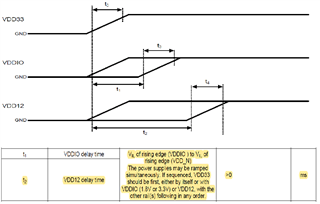
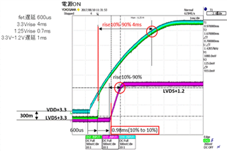
My customer checked their existing system which was designed based on the power up sequence shown in revision A.  They controlled VDD12 to start rising after VDD33 at 10% voltage level as shown below.  However the sequence has changed in revision D or between A and D which may violate the new requirement because VDD12 rose before VDD33 at 90% voltage level.  Would you please tell me if it does?

Best Regards,

Yoshikazu Kawasaki

  • Hi Yoshikazu,

    The requirement that VDD33 must rise before VDD12 has not changed since revision A. We cannot guarantee your system will work if datasheet requirements are not met.

    See the Power Up Requirements section from Revision A:


    Best Regards,

    Melissa

  • Hello Melissa-san,

    Thank you very much for your reply.  Please let me confirm the power up sequence of my customer's system.

    1.Violation for revision A

    As you mentioned the rise time of all the power supply pins needs to be faster than 1.5ms, but VDD33 took around 4ms.  It means the power up sequence of my customer's system already had violation for revision A.  Am I correct?

    2.Violation for revision D

    The rise time of VDD33 has changed from <1.5ms(max) to 0.2ms(min).  It means the power up sequence of my customer's system meets revision D for this since it took around 4ms.  However it has another violation, VDD33 to VDD12 delay which needs to be 0ms(min), but it is <-2ms.  Am I correct?

    Best Regards,

    Yoshikazu Kawasaki

  • Hello Yoshikazu-san,

    1. The datasheet requirement from Revision A I was referring to was that all inputs must not be driven HIGH until both VDD33 and VDDIO have reached steady state in section 10.1. This requirement has not changed from Revision A to Revision D. See the screenshot from Revision A below.

    2. Yes, it does not meet the requirement of the VDD33 to VDD12 delay. However, as I mentioned before, this was mentioned in Revision A in the paragraph above. It was just later added to the table in Revision D for further clarification.

    Best Regards,

    Melissa Chang

  • Hello Melissa-san,

    Thank you for your comments again. The datasheet in revision A says t2>0ms.  The t2 should be the time from 10%(or rising edge) of VDD33 to 10%(or rising edge) of VDD12.  Therefore my customer's system should meet the power up sequence required in revision A except VDD33 rise time(<1.5ms vs 4ms).  Am I wrong?  The sentence you showed doesn't say the exact voltage level.  It can be rising edge or 90%, but the table shown below doesn't look 90%, so I think my customer's system met the order requiring from VDD33 rail to VDD12 rail.  Would you please give me your comments again?

    Best Regards,

    Yoshikazu Kawasaki

  • Hello Yoshikazu-san,

    No problem. Section 10.1 from Revision A says that 'all inputs must not be driven until both VDD33 and VDDIO has reached steady state'. In the timing diagram you showed above, VDD12 is being driven while VDD33 is in transient state, not steady state.

    Best Regards,

    Melissa

  • Hello Melissa-san,

    I'm not talking about the input signals here in this thread since the plot I showed doesn't show any input signals, but doing only the sequence of VDD33 and VDD12.  The word you mentioned as "VDD12 is being driven while VDD33 is in transient state, not steady state" should also be for the input signals, not for VDD12 since the datasheet says "All inputs must not be driven until both VDD33 and VDDIO has reached steady state" and t2>0ms.  Therefore I understand the violations on my customer's system are the followings.  Am I correct?  Please let me confirm again.

    1.Violation for revision A

    As you mentioned the rise time of all the power supply pins needs to be faster than 1.5ms, but VDD33 took around 4ms.  It means the power up sequence of my customer's system already had violation for revision A.  The other items shown below are OK.  Am I correct?

    2.Violation for revision D

    The rise time of VDD33 has changed from <1.5ms(max) to 0.2ms(min).  It means the power up sequence of my customer's system meets revision D for this since it took around 4ms.  However it has another violation, VDD33 to VDD12 delay which needs to be 0ms(min) in revision D, but it is <-2ms on my customer's system.  It wasn't a violation in revision A, but it IS a violation in revision D.  Am I correct?  If I am, some customers should have violation for the power up sequence designed based on revision A.  Or do you think it's OK because it wasn't a violation for revision A datasheet?  Please give me your comments for this.

    Best Regards,

    Yoshikazu Kawasaki

  • Hello Yoshikazu-san,

    Please reference Revision D for the most correct and up-to-date power-up sequence requirements. Your customer's power-up sequence does not meet the VDD33 / VDDIO to VDD12 delay requirements from Revision D so we cannot guarantee it will work.

    Best Regards,

    Melissa Chang