This thread has been locked.

If you have a related question, please click the "Ask a related question" button in the top right corner. The newly created question will be automatically linked to this question.

SN65HVD37: About layout guideline

Part Number: SN65HVD37

Hi team.

My customer is designing the layout for SN65HVD37DR.

I guess they have to care about below:

  • Parallel/equal-length wiring for receiving side A, B and transmitting side Y, Z, respectively.
  • Receiver A,B and Transmitter Y,Z should not be too close. So, ensure creepage distance of at least twice the line width.
  • It is acceptable to set the receiver A, B and transmit Y and Z to L/S = 0.15mm/0.15mm respectively.
  • For MCU connection side R,D, creepage distance should be secured at least twice the line width, and equal length wiring is not preferred.

Is there any other tips for the layout guideline to reduce niose?

It will help if there are some collaterals that explains some tips for the layout for this device.

Regards,

Ohashi

  • Hi Ohashi-san,

    The tips you have right now look good. I have a few more guidelines to aid in the design of this system.

    1. A/B and Y/Z should be differentially coupled - i.e. the separation between A and B should be kept constant - and if they do need to increase or decrease the distance between them the increase/decrease should be symmetrical to keep the line lengths equal and to help mitigate noise. The same procedure should be applied to Y/Z.

    2. The trace characteristic impedance, cable characteristic impedance (if cabling is used), and the bus termination should be approximately equal - generally this is recommended to be 120 Ohms - mismatch will cause reflections. 

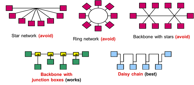
    3. If more than 2 devices are present on the bus the preferred topology is daisy chain or Spine with Junction boxes as shown below, along with 3 topologies that are not advisable:

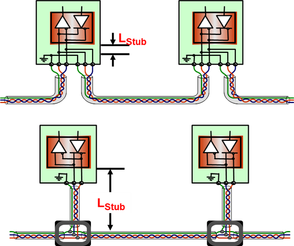
    4. If more than 2 nodes are present the stub length (deviation from main differential bus and non-terminal node) needs to follow the following guidelines (stub distance shown fro daisy chain and junction box respectively):

    So for this device when using the minimum transition time (3ns) and assuming v = 0.7 the max stub length is ~63mm after which you could start seeing noticeable reflections in the system. But typically when using the typical transition time (6ns) you will double it - but there is risk to doing that. 

    Since this device is faster daisy chain would be the preferred method to reduce reflection issues which would lead to potential noise issues.

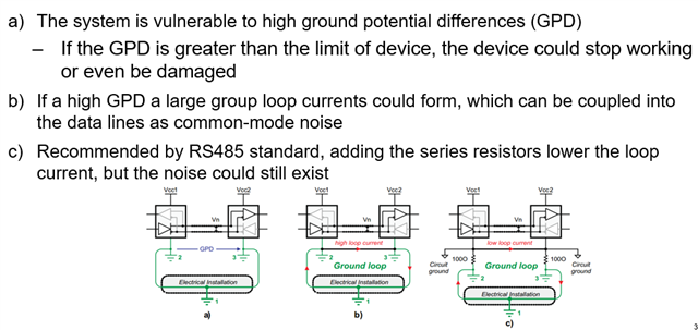
    5. The ground plane can become a noisy area of this circuit - so there is some general advise on lowering ground loop current and mitigating noise - this won't apply to every system but its still general advise.

    (this shows a half duplex device - but the same can be said of full duplex devices) 

    We don't have any specific collateral on layout guidelines for this device, our newer devices typically do in their datasheets but this device does not, but I would be more than happy to review layout if the customer ever wants TI to review it. 

    Please let me know if you have any other questions!

    Best,

    Parker Dodson