This thread has been locked.

If you have a related question, please click the "Ask a related question" button in the top right corner. The newly created question will be automatically linked to this question.

Issue about SN65LVDS307 and SN65LVDS310

Hi, I have a problem about the LVDS. I had used the LVDS ICs SN65LVDS307 and SN65LVDS310 to convert VGA data(clock is 6.5MHz). The SN65LVDS307 is the transmitter and SN65LVDS is the reciever.  The output LDVS signal of  transmitter is fine, clock is 6.5MHz,and |CLK+ - CLK-|=100mV. But reciever is not work.the enable signal, power of the reciever is fine.But the reciever not has output signals, clock and DE of the reciever are LOW,and others signals are HIGH.Please hlep me to work out this probelm.Thank you!

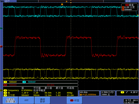
 The picture is the output signals of the transmitter.  Yellow is CLK+,blue is CLK- and Red is the value of  |CLK+ - CLK-|
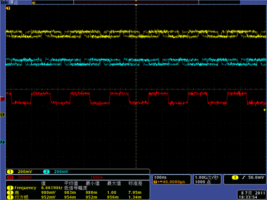
  • Hi Lorin,

    The most basic problem is that your LVDS receiver (LVDS310) isn't outputting a PCLK.  Please verify the RXEN input is 1.8V, and verify power/ground.  You could also try connecting an external clock generator to the LVDS310 CLK+- to see if it then outputs PCLK.

    Thanks,
    RE

  • Hi RossE,

      Thank you first. I have connected an external clock generator to the LVDS310 CLK+ and CLK- connected to groud. And my LVDS receiver was not output the PCLK. I had verified the RXEN input is 1.8V and power/groud is ture. I readed the Spec of LVDS307 that the value of Vod( |Vclk+ - Vclk-|) is 100mV~200mV, but my transmitter's Vod is 1000mV(see the picture,the RED is the Vod signal. And the test points are LVDS307's output pin,not through any resistances and capacitances). Is it ture?


    Thank you!

  • Hi Lorin,

    I saw you said "external clock generator to the LVDS310 CLK+ and CLK- connected to groud".  CLK- should not be connected to GND.  Ideally, you should use a differential clock generator and connect to both CLK+ and CLK-.  But if you don't have an external differential clock generator, I've found that it usually works to leave one LVDS310 CLK pin open and only drive the other CLK.  So you could try driving CLK+ with your clock, and leave CLK- unconnected.  As long as device PWR/GND is connected, and RXEN = 1.8V, the device should output PCLK.

    Yes, you can measure test points directly on the LVDS307 output.  If the outputs are not terminated through 50ohms to 0.9V (as they are in a real system), the voltages you measure might not match what you expect.  You might measure with a scope using 50ohms to GND, to see the waveform and Vod, and later when you connect the LVDS307 to LVDS310, you can use a High Impedance probe to measure the correct voltages.

    Thanks,
    RE

  • 1602.LVDS.pdfHi RossE,

    Thank you first. I had done the work follow you had said. And outputs of LVDS310 were not changed. The annex are the schematics of Transmitter board and Reciever board.

    Could you help me to check the schematics? Is there some wrong.Thanks!6278.LVDS.pdf

  • Hi Lorin, thanks for sending your schematic.  I noticed there are 50ohm series resistors (R32, R33, R34, R35).  These should not be there, and they should be replaced with 0ohm resistors.  TI Flatlink receivers have integrated 100ohm termination (Zdiff), as shown on Page 2 of the LVDS310 datasheet.

    Thanks,
    RE

  • Hi RossE,

      Thank you for the help. I try to debug it any kinds of methods, but not a good result. I think that I will with other LVDS IC. Do you know which LVDS IC suitable for 6.5MHz,27bit data of VGA ? Please tell me.  Thanks very much!

  • Hi Lorin, I'm sorry to hear that it still isn't working.  I really want to help you further.  If you'd like, I can obtain an EVM that's equivalent to the LVDS310, test it, verify the PCLK output, tell you my applied conditions, and ship you the EVM.  Our EVMs have SMA connectors on the LVDS lines and berg headers for the parallel.

    Do you think this could be helpful?  If so, please arrange this by emailing me directly at reisenbeis @ ti.com

    Thanks,
    RE