This thread has been locked.

If you have a related question, please click the "Ask a related question" button in the top right corner. The newly created question will be automatically linked to this question.

DS90UB949-Q1EVM: Can't select Enable Generator

Part Number: DS90UB949-Q1EVM
Other Parts Discussed in Thread: ALP, USB2ANY

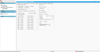
After connecting my DS90UB949 On pattern Generator tab i cant able to select Enable Generator check box. how to send my EDID for 854X480 resolution. Help me to resolve this issue.

Thanks 

  • Hello Sundar,

    1) If you are selecting External timing or External Clock, make sure you have a video source connected at the input of the UB949. Otherwise, select Internal.

    2) Also, if you change any parameter from the Video Control on the right-hand side, you have first to apply and then enable the Generator.

    3) If still not working, make sure to connect ALP only to one device, not two as shown.

  • Hey Thanks for your reply !

    Actually my issue is at initial stage while connecting UB949 with ALP tool Current link status is good as shown in below picture 

    After this if I select pattern generator tab or any other tab, UB926 not detecting. I don't understand this issue. Sometimes pattern generator tab itself not opening.

    Share the EDID memory table for 854X480 resolution. 

    Thanks 

    Sundar 

  • Hey Thanks for your reply !

    Actually my issue is at initial stage while connecting UB949 with ALP tool Current link status is good as shown in below picture 

    After that if I select pattern generator tab or any other tab, UB926 connection lost as show in the below picture. I don't understand this issue. Sometimes pattern generator tab itself not opening at this situation.

    Share the EDID memory table for 854X480 resolution . 

    Thanks 

    Sundar 

  • Hello Sundar,

    I can see you have a very similar questions in another thread. Hence, I am going to close this thread.

  • Hello Hamzeh,

    I Can't find any thread with similar question. Kindly guide us to solve this issue.

    Thanks

  • Now I can able to select pattern generator from registers settings.....But my output is flickering. I don't know where is the issue kindly help us to solve this.

    Regards

    Saravana

  • Hello Sundar,

    which type of Pattern generator are you using? Can you post a screen shot from the Patgen Tab ?

  • EDID write is done and its working properly. 

    Now we have another requirement to write EDID via UART in the same DS90UB949 EVM. Kindly suggest writing EDID via UART is possible. Kindly mention the addresses to write EDID.

    Thanks

  • Hello Sundar,

    The process for writing the EDID SRAM is as follows:


    1) Set Reg 0x48[0] to enable APB. This bit should remain set through remainder of procedure. Reg 0x48[4:3] should be set to 01. If desired, the auto increment bit (Reg 0x48[2]) may be set to enable the auto-increment function.

    2) Write to Reg 0x49 to set the 8-bit register address.

    3) Write the 8-bit data to Reg 0x4B. The APB Interface write will occur once this register has been written.

    4) If APB auto increment bit is set, the next register location may be written by repeating step 2, otherwise repeat steps 1 and 2 to write another register location.

    Additionally, please refer to this Thread and this Thread.

  • Hi Hamzeh 

    Ta

    Thanks for your support.

    1. I connected UART to J23 located in the DS90UB949 EVM board schematics(Page No: 39) as shown in the below picture. Is that connection is correct ?

    https://www.ti.com/lit/ug/snlu169/snlu169.pdf?ts=1683119460784&ref_url=https%253A%252F%252Fwww.google.com.hk%252F 

    2. If UART connection is correct then suggest any other register setting is required before writing EDID.

    Regards

    Saravanakumar D

  • Hello Sundar,

    we never used UART for this application. We use I2C only. 

  • Thanks!!!

    1. Can you specifically mention where to connect my IIC and give required register settings to get proper output. 

    2. We have requirement  like [PC USB->UART ->EVM MCU MSP430->IIC-> EVM SER UB949->FPD III->DESER UB926->HUD MCU]. Will you confirm by checking this UART communication.

    Regards

    Saravanakumar D 

  • On the UB949 EVM, you would need to connect your I2C to either I2C headers or to the DDC headers shown in the screenshot below.


    1) Accessing EDID SRAM via I2C
    • EDID SRAM data is accessible from the I2C interface on the device through an indirect register access mechanism provided by the APB Interface registers.
    • The APB Interface registers consist of a control register (Reg 0x48), address registers (Reg 0x49, 0x4A) and data registers (Reg 0x4B – 0x4E).
    • The address registers provide the byte offset to the EDID SRAM.
    • When accessing EDID SRAM, only the first data register (Reg 0x4B) is used since the interface is 8-bits.
    • For EDID SRAM accesses, Reg 0x48[4:3] should be set to a value of 01 to select EDID SRAM.

    The process for writing the EDID SRAM is as follows:
    1) Set Reg 0x48[0] to enable APB. This bit should remain set through remainder of procedure. Reg 0x48[4:3] should be set to 01. If desired, the auto increment bit (Reg 0x48[2]) may be set to enable the auto-increment function.
    2) Write to Reg 0x49 to set the 8-bit register address.
    3) Write the 8-bit data to Reg 0x4B. The APB Interface write will occur once this register has been written.
    4) If APB auto increment bit is set, the next register location may be written by repeating step 2, otherwise repeat steps 1 and 2 to write another register location.

    The process for reading EDID SRAM is as follows:
    1) Write to Reg 0x49 to set the 8-bit register address.
    2) Set Reg 0x48[1]. This will initiate the APB Interface read. Reg 0x48[0] must also be set during any write to reg 0x48, while the Reg 0x48[4:3] must be set to 01. If desired, the APB auto increment bit (Reg 0x48[2]) may be set to enable the auto-increment function.
    3) Read the first APB data register (Reg 0x4B).
    4) If APB auto increment bit was set, the next register location may be read by repeating steps 2 and 3, otherwise repeat steps 1-3 to read another register location.
    ----------------------

    2) Reading EDID SRAM via DDC:
    • The HDMI DDC interface is a simple I2C interface which allows access to the EDID information for an upstream HDMI Transmitter.
    • After initialization, if the DDC interface is enabled, the 256-byte EDID structure can be read using the DDC interface directly.
    • By default the EDID structure will be located at a slave address of 0xA0 (8-bit address). This address location can be changed by changing the value in Reg 0x51.
    • By default the interface is read-only, but can be made writable by clearing bit 0 of Reg 0x51.
    • The interface is a standard I2C slave interface capable at operating with Standard-mode or Fast-mode timing.
    • The DDC interface to the EDID SRAM can be disabled by setting Reg 0x4F[0].

  • Thanks Hamzeh

    What about UART communication? in EVM we have UART header pins available, I think by changing some register setting in MSP430 we can access UART. kindly clarify why UART is provided in J23 Header.

    As per the EVM schematics this I2C is directly connected to UB949 right ? Do you have any specific I2C tool to write into registers ?

    Regards

    Saravanakumar D

  • Sundar,

    you can use UART but not for writing or reading EDID. This can be accessed only via I2C or DDC buses.

  • Hamzeh,

    Is there any specific tool to write I2C ?

  • You can either connect your I2C USB2ANY or Aardvark tools to the I2C bus, or you can simply connect your PC via USB cable to the Mini-USB connector on the board and use the embedded MSP430 microcontroller to interface with the UB949.