This thread has been locked.

If you have a related question, please click the "Ask a related question" button in the top right corner. The newly created question will be automatically linked to this question.

DS90UB960-Q1: Test pattern generation

Part Number: DS90UB960-Q1
Other Parts Discussed in Thread: ALP

Hi Team,

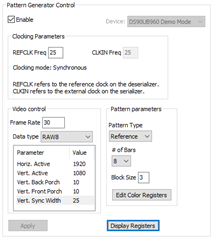
We are using ds90ub960-q1 to generate a test pattern refer to 7.5.12.4 of datesheet. We are not able to capture the test pattern. We see that the v4l2-ctl is select timeout and it is not getting any frame. The trace log shows that the LP sequence is error.

The relevant register configuration is as follows:

  • CSI_PORT_SEL(0x32): 0x01
  • FWD_CTL1(0x20): 0xF0
  • CSI_PLL_CTL(0x1F): 0x02
  • CSI_CTL1(0x33): 0x01

So what should be the values of cil_settletime and serdes_pix_clk_hz?

  • Hi Wenqiang,

    Can I get the initiation code for the 960? Was the FWD_CTL2 Register (0x21) set-up correctly?

    What is the test pattern they need? Please provide the following and I can provide the registers.

    PATGEN Output   
       
    Horizontal Resolution 1920
    Vertical  Resolution 720
    Total Vertical Blanking  182
    Vertical Front Porch 2
    Vertical Back Porch 29
    Vertical Sync  151
    Frame Rate 30
    FC Rate 2.528
    Data type Raw12

    Glenn 

  • Hello Glenn Uranga,

    I did not configure 0x21 and used the default value 0x03. As I said, I used the configuration in chapter 7.5.12.4 of the datasheet.

    static int pattern_generator(struct regmap *map)
    {
    int err = 0;

    TRY(err, regmap_write(map, 0xB0, 0x0));

    TRY(err, regmap_write(map, 0xB1, 0x01)); // PGEN_CTL
    TRY(err, regmap_write(map, 0xB2, 0x01)); // enagle PGEN

    TRY(err, regmap_write(map, 0xB1, 0x02)); // PGEN_CFG
    TRY(err, regmap_write(map, 0xB2, 0x33)); // Send Color Bar Pattern, 4 Color Bars, 4 bytes

    TRY(err, regmap_write(map, 0xB1, 0x03)); // PGEN_CSI_DI
    TRY(err, regmap_write(map, 0xB2, 0x24)); // 0x24:RGB888 0x2A:RAW8 0x2E:RAW16

    TRY(err, regmap_write(map, 0xB1, 0x04)); // PGEN_LINE_SIZE1
    TRY(err, regmap_write(map, 0xB2, 0x0f)); // 0xf00 = 3840 = 1280 x 3
    TRY(err, regmap_write(map, 0xB1, 0x05)); // PGEN_LINE_SIZE0
    TRY(err, regmap_write(map, 0xB2, 0x00)); //

    TRY(err, regmap_write(map, 0xB1, 0x06)); // PGEN_BAR_SIZE1
    TRY(err, regmap_write(map, 0xB2, 0x01)); // 0x1e0 = 480
    TRY(err, regmap_write(map, 0xB1, 0x07)); // PGEN_BAR_SIZE0
    TRY(err, regmap_write(map, 0xB2, 0xe0)); //

    TRY(err, regmap_write(map, 0xB1, 0x08)); // PGEN_ACT_LPF1
    TRY(err, regmap_write(map, 0xB2, 0x02)); // 0x2d0 = 720
    TRY(err, regmap_write(map, 0xB1, 0x09)); // PGEN_ACT_LPF0
    TRY(err, regmap_write(map, 0xB2, 0xd0)); //

    TRY(err, regmap_write(map, 0xB1, 0x0a)); // PGEN_TOT_LPF1
    TRY(err, regmap_write(map, 0xB2, 0x04)); // 0x41a = 1050
    TRY(err, regmap_write(map, 0xB1, 0x0b)); // PGEN_TOT_LPF0
    TRY(err, regmap_write(map, 0xB2, 0x1a)); //

    TRY(err, regmap_write(map, 0xB1, 0x0c)); // PGEN_LINE_PD1
    TRY(err, regmap_write(map, 0xB2, 0x0c)); // 0xc67 = 3175
    TRY(err, regmap_write(map, 0xB1, 0x0d)); // PGEN_LINE_PD0
    TRY(err, regmap_write(map, 0xB2, 0x67)); //

    TRY(err, regmap_write(map, 0xB1, 0x0e)); // PGEN_VBP
    TRY(err, regmap_write(map, 0xB2, 0x21)); //
    TRY(err, regmap_write(map, 0xB1, 0x0f)); // PGEN_VFP
    TRY(err, regmap_write(map, 0xB2, 0x0A)); //

    return err;
    }

    PATGEN Output   
       
    Horizontal Resolution 1280
    Vertical  Resolution 720
    Total Vertical Blanking  330
    Vertical Front Porch 10
    Vertical Back Porch 33
    Vertical Sync  ?
    Frame Rate 30
    FC Rate ?
    Data type RGB888

    What is FC Rate? 

    If the above configuration is used, what parameters should be passed to v4l2-ctl to read data?

  • HI Wenqiang,

    FC is forward channel rate. I assumed you are using 4.16Gbps for the calculations below. 

    I haven't worked on the v4l2-ctl before so not sure how to set that up. With the patgen you provided above the image is as follows:

    PATGEN Output   
       
    Horizontal Resolution 1280
    Vertical  Resolution 720
    Total Vertical Blanking  330
    Vertical Front Porch 10
    Vertical Back Porch 33
    Vertical Sync  287
    Frame Rate 30
    Data Type RGB888

    With this information is what we use to setup our decoder. 


    I also have a script bellow that issued in the past for testing purposes. It uses the following patgen output. I am using the 960 to sent the patgen but I can change it to the 960 patgen. Let me know if you want me to change it to 960 patgen. Note in the code you will see 954 but this works for 960 as well. 

    PATGEN Output   
       
    Horizontal Resolution 1920
    Vertical  Resolution 1080
    Total Vertical Blanking  45
    Vertical Front Porch 10
    Vertical Back Porch 33
    Vertical Sync  2
    Frame Rate 31
    Video format YUV422 8-bit


    """
      Copyright 2018 Texas Instruments Incorporated. All rights reserved.
    
      IMPORTANT: Your use of this Software is limited to those specific rights
      granted under the terms of a software license agreement between the user who
      downloaded the software, his/her employer (which must be your employer) and
      Texas Instruments Incorporated (the "License"). You may not use this Software
      unless you agree to abide by the terms of the License. The License limits your
      use, and you acknowledge, that the Software may not be modified, copied or
      distributed unless embedded on a Texas Instruments microcontroller which is
      integrated into your product. Other than for the foregoing purpose, you may
      not use, reproduce, copy, prepare derivative works of, modify, distribute,
      perform, display or sell this Software and/or its documentation for any
      purpose.
    
      YOU FURTHER ACKNOWLEDGE AND AGREE THAT THE SOFTWARE AND DOCUMENTATION ARE
      PROVIDED AS IS WITHOUT WARRANTY OF ANY KIND, EITHER EXPRESS OR IMPLIED,
      INCLUDING WITHOUT LIMITATION, ANY WARRANTY OF MERCHANTABILITY, TITLE,
      NON-INFRINGEMENT AND FITNESS FOR A PARTICULAR PURPOSE. IN NO EVENT SHALL TEXAS
      INSTRUMENTS OR ITS LICENSORS BE LIABLE OR OBLIGATED UNDER CONTRACT,
      NEGLIGENCE, STRICT LIABILITY, CONTRIBUTION, BREACH OF WARRANTY, OR OTHER LEGAL
      EQUITABLE THEORY ANY DIRECT OR INDIRECT DAMAGES OR EXPENSES INCLUDING BUT NOT
      LIMITED TO ANY INCIDENTAL, SPECIAL, INDIRECT, PUNITIVE OR CONSEQUENTIAL
      DAMAGES, LOST PROFITS OR LOST DATA, COST OF PROCUREMENT OF SUBSTITUTE GOODS,
      TECHNOLOGY, SERVICES, OR ANY CLAIMS BY THIRD PARTIES (INCLUDING BUT NOT
      LIMITED TO ANY DEFENSE THEREOF), OR OTHER SIMILAR COSTS.
    
      Should you have any questions regarding your right to use this Software,
      contact Texas Instruments Incorporated at www.TI.com.
    
    """
    # Patgen YUV422 8-bit ColorBar  1920x1080p30 on 953/954
    
    
    import time
    
    Alias953 = 0x30
    DES954 = 0x7a #works with 960 
    
    
    # Reset 954
    board.WriteI2C(DES954, 0x01, 0x01)
    time.sleep(1.0)
    board.WriteI2C(DES954, 0x20,0xF0) # Disable fowarding
    #CSI Port Sel
    board.WriteI2C(DES954, 0x32, 0x01)
    # CSI enable
    board.WriteI2C(DES954, 0x33, 0x01)
    time.sleep(0.1)
    # Set CSI_TX_SPEED 
    board.WriteI2C(DES954, 0x1F, 0x02)
    time.sleep(0.1)
    # Port Control
    board.WriteI2C(DES954, 0x0C, 0x0F)
    time.sleep(0.1)
    # Port Selection
    board.WriteI2C(DES954, 0x4C, 0x01)
    time.sleep(0.1)
    # set alias
    board.WriteI2C(DES954, 0x5C, Alias953)
    time.sleep(0.1)
    board.WriteI2C(DES954, 0x20,0x00) # forwarding of all RX to CSI0
    time.sleep(0.1)
    
    
    # Reset 953
    board.WriteI2C(Alias953, 0x01, 0x01)
    time.sleep(1.0)	
    # enable pat gen
    board.WriteI2C(Alias953, 0xB0, 0x00)
    board.WriteI2C(Alias953, 0xB1, 0x01)
    board.WriteI2C(Alias953, 0xB2, 0x01) #enable pattern generator
    print "Enable PatGen"
    
    board.WriteI2C(Alias953, 0xB1, 0x02)
    board.WriteI2C(Alias953, 0xB2, 0x33) #fixed color pattern, 8 color bars, block size of 5
    
    board.WriteI2C(Alias953, 0xB1, 0x03)
    board.WriteI2C(Alias953, 0xB2, 0x1E) #CSI Data Identifier (0x24 = RGB888, 0x2C = RAW12, 0x2B = RAW10)
    
    board.WriteI2C(Alias953, 0xB1, 0x04)
    board.WriteI2C(Alias953, 0xB2, 0x0f) #line size (15:8)
    
    board.WriteI2C(Alias953, 0xB1, 0x05)
    board.WriteI2C(Alias953, 0xB2, 0x00) #line size (7:0)
    
    board.WriteI2C(Alias953, 0xB1, 0x06)
    board.WriteI2C(Alias953, 0xB2, 0x01) #bar size (15:8)
    
    board.WriteI2C(Alias953, 0xB1, 0x07)
    board.WriteI2C(Alias953, 0xB2, 0xe0) #bar size (7:0)
    
    board.WriteI2C(Alias953, 0xB1, 0x08)
    board.WriteI2C(Alias953, 0xB2, 0x04) #active lines per frame (15:8)
    
    board.WriteI2C(Alias953, 0xB1, 0x09)
    board.WriteI2C(Alias953, 0xB2, 0x38) #active lines per frame (7:0)
    
    board.WriteI2C(Alias953, 0xB1, 0x0a)
    board.WriteI2C(Alias953, 0xB2, 0x04) #total lines per frame (15:8)
    
    board.WriteI2C(Alias953, 0xB1, 0x0b)
    board.WriteI2C(Alias953, 0xB2, 0x65) #total lines per frame (7:0)
    
    board.WriteI2C(Alias953, 0xB1, 0x0c)
    board.WriteI2C(Alias953, 0xB2, 0x0b) #line period (15:8)
    
    board.WriteI2C(Alias953, 0xB1, 0x0d)
    board.WriteI2C(Alias953, 0xB2, 0x93) #line period (7:0)
    
    board.WriteI2C(Alias953, 0xB1, 0x0e)
    board.WriteI2C(Alias953, 0xB2, 0x21) #vertical back porch
    
    board.WriteI2C(Alias953, 0xB1, 0x0f)
    board.WriteI2C(Alias953, 0xB2, 0x0a) #vertical front porch
    

  • Hello Glenn Uranga,

    The value of the register CSI_PLL_CTL (0x1F) is set to 0x02, which means that the FC Rate is 800 Mbps.

    "Figure 6-5. Clock and Data Timing in HS Transmission" of DS90UB960-Q1 datasheet shows the measurement method of UI. I understand that the time between two crossings of the two clock lines is 1UI. According to this understanding, the measured UI is 1.2ns, and the calculated value range of cil_settletime is "13<= cil_settletime <= 26". But I still get the log "LP sequence error". Is my measurement of UI wrong?

    If we adjust the LP sequence instead of cil_settletime but mclk_multiplier, how do we determine the value of mclk_multiplier?

    If you could tell me the correct way to measure the UI or a way to determine the value of mclk_multiplier, I would be very grateful to you.

    The definitions of cil_settletime and mclk_multiplier can be found at https://docs.nvidia.com/jetson/archives/r35.2.1/DeveloperGuide/text/SD/CameraDevelopment/SensorSoftwareDriverProgramming.html#sensor-pixel-clock

  • Wenquiang,

    let me look into this for you. Allow a few days.

    Glenn 

  • Hi Wenquiang,

    Your calculation for cil_settletime looks correct, I calculated it as well and got the same result. UI_INST = 1 / CSI data rate (800Mbps in your case) = 1.25ns.

    mclk_multiplier = desired ISP clock frequency in hertz / mclk, where the desired ISP clock frequency is your CSI data rate 800Mbps/2 = 400MHz and mclk is your reference clock, which I'm assuming is 25MHz. Based on this, mclk_multiplier = 16.

    Given that we have never used this system v4l2-ctl before, we are unsure why you are getting LP sequence errors.

    Best,

    Lucas

  • Hi Wenquiang,

    I just thought of one more thing. Are you using continuous or discontinuous clock? And is the boolean variable discontinuous_clk on your v4l2 framework set correctly?

    Best,

    Lucas

  • Hi Lucas Wolter,

    Thank you for your reply.

    “CSI_CTL(0x33): 0x01” means that the UB960 uses a discontinuous clock.

    If you don't use v4l2-ctl, what linux tool do you use to read the raw data of the sensor?

    Is the value set by the CSI_PLL_CTL register (0x1F) the data rate of a data lane?

    The clock of output of sensor in my solution is continuous. I set the clock of serializer UB953 to continuous and UB960 to non-continuous. Can this configuration work properly?

  • Hi Wenqiang,

    If you don't use v4l2-ctl, what linux tool do you use to read the raw data of the sensor?

    We use Analog Launchpad, which is a GUI developed by TI to debug our FPD serializers and deserializers.

    We also use these Introspect products.

    Is the value set by the CSI_PLL_CTL register (0x1F) the data rate of a data lane?

    Yes that's correct.

    The clock of output of sensor in my solution is continuous. I set the clock of serializer UB953 to continuous and UB960 to non-continuous. Can this configuration work properly?

    Yes, this configuration will work as long as the grabber does not feed back into the SER.

    Best,

    Lucas

  • Hi Lucas Wolter,

    Thank you for your reply.

    If the following format is used for testing, which registers need to be configured?

    The resolution of effective image data is 1920*1080, but what is the original resolution of the read raw data?

    board.WriteReg(0x33, 0x03)
    
    board.WriteReg(0xB0, 0x02) # IA_AUTO_INC=1
    board.WriteReg(0xB1, 0x01) # PGEN_CTL
    
    board.WriteReg(0xB2, 0x01) # PGEN_ENABLE=1
    board.WriteReg(0xB2, 0x33) # PGEN_CFG
    board.WriteReg(0xB2, 0x2A) # PGEN_CSI_DI
    board.WriteReg(0xB2, 0x07) # PGEN_LINE_SIZE1
    board.WriteReg(0xB2, 0x80) # PGEN_LINE_SIZE0
    board.WriteReg(0xB2, 0x00) # PGEN_BAR_SIZE1
    board.WriteReg(0xB2, 0xF0) # PGEN_BAR_SIZE0
    board.WriteReg(0xB2, 0x04) # PGEN_ACT_LPF1
    board.WriteReg(0xB2, 0x38) # PGEN_ACT_LPF0
    board.WriteReg(0xB2, 0x04) # PGEN_TOT_LPF1
    board.WriteReg(0xB2, 0x65) # PGEN_TOT_LPF0
    board.WriteReg(0xB2, 0x0B) # PGEN_LINE_PD1
    board.WriteReg(0xB2, 0x93) # PGEN_LINE_PD0
    board.WriteReg(0xB2, 0x0A) # PGEN_VBP
    board.WriteReg(0xB2, 0x0A) # PGEN_VFP
    board.WriteReg(0xB2, 0xAA) # PGEN_COLOR0
    board.WriteReg(0xB2, 0x33) # PGEN_COLOR1
    board.WriteReg(0xB2, 0xF0) # PGEN_COLOR2
    board.WriteReg(0xB2, 0x7F) # PGEN_COLOR3
    board.WriteReg(0xB2, 0x55) # PGEN_COLOR4
    board.WriteReg(0xB2, 0xCC) # PGEN_COLOR5
    board.WriteReg(0xB2, 0x0F) # PGEN_COLOR6
    board.WriteReg(0xB2, 0x80) # PGEN_COLOR7
    board.WriteReg(0xB2, 0x00) # PGEN_COLOR8
    board.WriteReg(0xB2, 0x00) # PGEN_COLOR9
    board.WriteReg(0xB2, 0x00) # PGEN_COLOR10
    board.WriteReg(0xB2, 0x00) # PGEN_COLOR11
    board.WriteReg(0xB2, 0x00) # PGEN_COLOR12
    board.WriteReg(0xB2, 0x00) # PGEN_COLOR13
    board.WriteReg(0xB2, 0x00) # PGEN_COLOR14
    board.WriteReg(0xB2, 0x00) # Reserved

  • Hi Wenqiang,

    This register configuration corresponds to the following patgen settings:

    If you have Analog Launchpad, you can configure the patgen registers using the "Pattern Generator" tab which looks like above. If you do not have ALP, you can tell me which values you want to configure for each parameter in the screenshot above and I can generate the register values for you.

    Best,

    Lucas

  • Hi Lucas,

    Thank you fro your reply!

    I don't have ALP, I want to know besides configuring the image format, do I need to configure other registers (except CSI_PORT_SEL, FWD_CTL1, CSI_PLL_CTL and CSI_CTL)? How must the CSI at the receiving end be configured to receive data correctly?

    If I follow my configuration above, what is the resolution of the received raw data?

  • Hi Wenqiang,

    No additional register configurations are necessary to receive the patgen data. The resolution of the received raw data will be 1920 bytes x 1080 lines.

    Best,

    Lucas

  • Hi Lucas,

    Thank you fro your reply!

    I have four questions that I need your help with.

    1. The value of PGEN_LINE_PD is set to 0x0B93, how is this value calculated?
    2. PGEN_TOT_LPF is set to 0x0465, do we not need to consider it when receiving data? Only read 1080 lines? When is that extra row discarded?
    3. How do the values of PGEN_VBP and PGEN_VFP come from? Can it be set to 0? What is the effect?
    4. If I want to set the data to 4096x512p10 and the format is still RAW8, what values should I set to PGEN_TOT_LPF, PGEN_LINE_PD, PGEN_VBP, PGEN_VFP?
  • Hi Wenqiang,

    1. PGEN_LINE_PD is the line period in 10ns units. 1/frame rate gives you the frame period, then divide by total number of lines to get the line period. For the configuration you gave above, 1 / 30fps / 1125 total lines = 29.63us = 2963 (10ns units) = 0xB93.
    2. The deserializer will automatically detect the vertical front porch, back porch, and sync lines and remove them from active frame pixels.
    3. Vertical front porch, back porch, and sync values are set by your imager. When using patgen for testing purposes, you can set these to any value including 0.
    4. What do you mean by p10 in the resolution? What framerate, vertical front porch, vertical back porch, and vertical sync values do you want to use? If you provide these values I can give you all of the patgen register values.


    Best,

    Lucas

  • Hi Lucas,

    Thank you fro your reply!

    p10 represents 10 frames. In my solution, the sensor is a radar. There are 1024 sampling points in one line, and one point is stored in 32 bits, so RAW8 is used for transmission. I can read data at a resolution of 4096*512, and then convert it to 1024*512. In this case, I still don't understand how to configure PGEN_CFG and PGEN_BAR_SIZE. The values of PGEN_VBP and PGEN_VFP are 0, how does vertical sync reflect in the pattern generator?

  • Hi Wenqiang,

    Does your radar sensor use CSI-2 packet format? This is a requirement to use 960/953. Just so I understand, the sensor data is getting sent through the 953 and 960 at a resolution of 4096x512 with RAW8 encoding? And then getting converted to 1024x512 after the 960?

    The PGEN_CFG and PGEN_BAR_SIZE registers configure the image that is being created by patgen. You can set them to any valid value, or leave the default values. My apologies, although the vertical front porch can be zero, the back porch does need some nonzero value. The reason is there is some buffer time needed in order to process each horizontal line.

    Best,

    Lucas